Enhanced GaN-based HEMT device and preparation method and application thereof

An enhanced, device technology, used in semiconductor/solid-state device manufacturing, semiconductor devices, electric solid-state devices, etc., can solve problems such as increasing manufacturing costs and reducing yields, avoiding gate degradation problems, and avoiding process complexity. increased effect

Pending Publication Date: 2022-05-10
NINGBO INST OF MATERIALS TECH & ENG CHINESE ACADEMY OF SCI
View PDF0 Cites 0 Cited by
  • Summary
  • Abstract
  • Description
  • Claims
  • Application Information

AI Technical Summary

Problems solved by technology

This is incompatible with the fabrication process of depletion-mode HEMT devices, so integration between depletion-mode and enhancement-mode HEMT devices tends to increase fabrication costs and reduce yield

Method used


Image

  • Enhanced GaN-based HEMT device and preparation method and application thereof
  • Enhanced GaN-based HEMT device and preparation method and application thereof
  • Enhanced GaN-based HEMT device and preparation method and application thereof

Examples


Embodiment 1

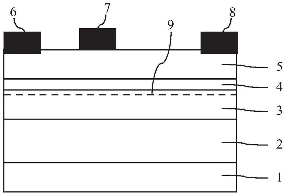
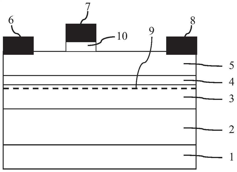
[0062] see image 3 As shown, an enhanced GaN-based HEMT device includes a sapphire substrate 1 and a GaN buffer layer 2, a GaN channel layer 3, an AlN insertion layer 4 and an AlGaN barrier layer 5 sequentially arranged on the sapphire substrate 1, A two-dimensional electron gas 9 is formed under the surface of the GaN channel layer 3 close to the AlN insertion layer 4 . The source 6 and the drain 8 are formed on the AlGaN barrier layer 5 and can be electrically connected through the two-dimensional electron gas 9, and an AlScN ferroelectric layer 10, the gate 7 is formed on the AlScN ferroelectric layer 10.

[0063] Further, a method for preparing an enhanced GaN-based HEMT device specifically includes:

[0064] 1) Provide a sapphire substrate 1, and sequentially epitaxially grow a GaN buffer layer 2 with a thickness of 5 μm, a GaN channel layer 3 with a thickness of 500 nm, and an AlN insertion layer with a thickness of 1 nm on the sapphire substrate 1 by metal-organic va...

Embodiment 2

[0074] The structure of the device in this embodiment is the same as that in Embodiment 1 image 3 The device structures shown are consistent, and the preparation method provided by it is also similar to the preparation method provided in Example 1, the difference is that the content of the Al component and the content of the Sc component of the ferroelectric layer 10 are changed, and another difference is The reason is that the thicknesses of the buffer layer and the channel layer are adjusted, which specifically include:

[0075] 1) Provide a sapphire substrate 1, and sequentially epitaxially grow a GaN buffer layer 2 with a thickness of 10 μm, a GaN channel layer 3 with a thickness of 10 nm, and an AlN insertion layer with a thickness of 1 nm on the sapphire substrate 1 by metal-organic vapor phase epitaxy 4 and Al with a thickness of 25nm 0.3 Ga 0.7 N barrier layer 5, wherein a two-dimensional electron gas 9 is formed under the surface of the GaN channel layer 3 close to...

Embodiment 3

[0085] see Figure 10 As shown, an enhancement mode GaN-based HEMT device with a fin structure is similar to the device structure in Embodiment 1, the difference is that it includes a sapphire substrate 1 and a GaN buffer layer 2 sequentially arranged on the sapphire substrate 1 , a GaN channel layer 3, an AlN insertion layer 4 and an AlGaN barrier layer 5, wherein the GaN channel layer 3, the AlN insertion layer 4 and the AlGaN barrier layer 5 cooperate to form a fin structure, and the GaN channel layer 3 is close to the AlN A two-dimensional electron gas 9 is formed under the surface of the insertion layer 4, and the gate 7 covers the channel region of the fin structure, that is, the region where the two-dimensional electron gas 9 is formed, and the gate 7 and the trench of the fin structure A ferroelectric layer 10 is arranged between the track regions.

[0086] Further, a method for fabricating an enhanced GaN-based HEMT device with a fin structure specifically includes: ...


PUM

PropertyMeasurementUnit
thicknessaaaaaaaaaa
thicknessaaaaaaaaaa
thicknessaaaaaaaaaa

Abstract

The invention discloses an enhanced GaN-based HEMT (High Electron Mobility Transistor) device as well as a preparation method and application thereof. The HEMT device comprises an epitaxial structure, the epitaxial structure comprises a first semiconductor layer and a second semiconductor layer arranged on the first semiconductor layer, and two-dimensional electron gas is formed between the first semiconductor layer and the second semiconductor layer; the source electrode, the drain electrode and the grid electrode are formed on the second semiconductor layer, the source electrode and the drain electrode can be electrically connected through the two-dimensional electron gas, and the grid electrode is distributed between the source electrode and the drain electrode; wherein a ferroelectric layer is also arranged between the grid electrode and the second semiconductor layer, the ferroelectric layer is formed by a hexagonal crystal ferroelectric material, and the ferroelectric layer is at least used for exhausting two-dimensional electron gas below the grid electrode, so that the enhancement function of the HEMT device and the regulation and control of threshold voltage are realized. The enhanced GaN-based HEMT device prepared by combining the hexagonal crystal form ferroelectric material provided by the invention is good in threshold voltage stability and simple in preparation process.

Description

technical field [0001] The invention belongs to the technical field of semiconductor devices, and relates to an enhanced GaN-based HEMT device, its preparation method and application. Background technique [0002] Compared with traditional silicon-based materials, gallium nitride (GaN) has the advantages of large band gap, high breakdown field strength, low dielectric constant, high electron saturation velocity and low on-resistance. High electron mobility transistors (HMETs) based on GaN materials generate high two-dimensional electron gas through spontaneous polarization and piezoelectric polarization, and have been widely used in high-power electronic devices, high-frequency microwave devices and other fields. [0003] Conventional GaN-based HEMT devices such as figure 1 As shown, since the conduction band at the AlGaN / AlN / GaN interface is below the Fermi energy, see figure 2 As shown, two-dimensional electron gas is generated, and the formed two-dimensional electron g...

Claims


Application Information

Patent Timeline
Patent Type & Authority Applications(China)
IPC IPC(8): H01L29/778H01L21/335H01L27/085H01L29/51
CPCH01L29/7787H01L29/516H01L29/66462H01L27/085
Inventor 郭炜赵紫辉叶继春
Owner NINGBO INST OF MATERIALS TECH & ENG CHINESE ACADEMY OF SCI
Why Eureka
Try Eureka