Method for taking crystal grains from backside illuminated CMOS (complementary metal oxide semiconductor) sensor and application

A CMOS sensor, back-illuminated technology, applied in the field of CMOS sensors, can solve the problem of not being able to take a complete grain, and achieve the effect of improving imaging quality, increasing speed, high sensitivity and signal-to-noise ratio

Pending Publication Date: 2022-05-13
GIGA FORCE ELECTRONICS CO LTD
View PDF18 Cites 0 Cited by
  • Summary
  • Abstract
  • Description
  • Claims
  • Application Information

AI Technical Summary

Problems solved by technology

[0005] The first object of the present invention is to provide a method for taking crystal grains in a back-illuminated

Method used


Image

  • Method for taking crystal grains from backside illuminated CMOS (complementary metal oxide semiconductor) sensor and application
  • Method for taking crystal grains from backside illuminated CMOS (complementary metal oxide semiconductor) sensor and application
  • Method for taking crystal grains from backside illuminated CMOS (complementary metal oxide semiconductor) sensor and application

Examples


Embodiment 1

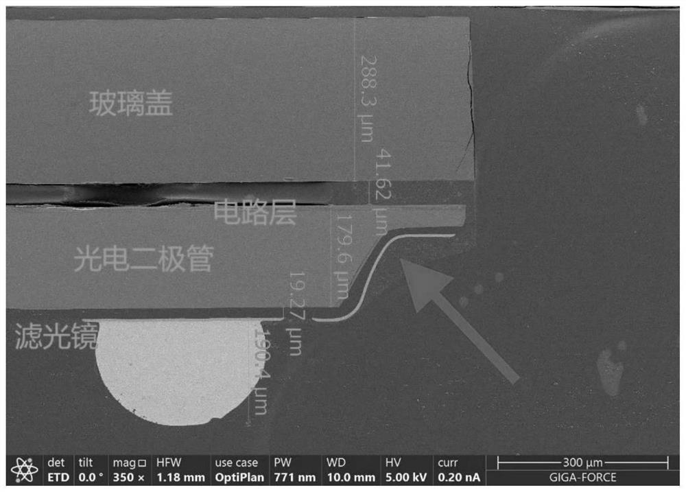
[0096] This embodiment provides a method for taking crystal grains in a back-illuminated CMOS sensor, comprising the following steps:

[0097] (a) placing the back-illuminated CMOS sensor in mixed acid for treatment to remove at least most of the packaging material on the surface of the grain, and taking it out to obtain a pre-treated grain;

[0098] Wherein, the mixed acid includes sulfuric acid and nitric acid, the mass fraction of sulfuric acid is 98%, the mass fraction of nitric acid is 68%, the volume ratio of sulfuric acid and nitric acid is 5:1, the treatment temperature is 150°C, and the treatment time is 1h;

[0099] (b) Apply glue (AB glue for preparing metal pattern samples, high temperature resistance temperature is 220°C) on the silicon wafer, and fix the side of the pretreated grain close to the circuit layer on the silicon wafer (can be used at 100°C Bake for 40 minutes to solidify), to ensure that there are no air bubbles between the pre-treated grains and the ...

Embodiment 2

[0105] This embodiment provides a method for obtaining crystal grains in a back-illuminated CMOS sensor. Except that the volume ratio of sulfuric acid and nitric acid in the mixed acid in step (a) is 4.5:1, the remaining steps and process parameters are the same as in Embodiment 1.

Embodiment 3

[0107] This embodiment provides a method for obtaining crystal grains in a back-illuminated CMOS sensor. Except that the volume ratio of sulfuric acid and nitric acid in the mixed acid in step (a) is 4:1, the remaining steps and process parameters are the same as in Embodiment 1.


PUM

PropertyMeasurementUnit
High temperature resistanceaaaaaaaaaa
Thicknessaaaaaaaaaa
Thicknessaaaaaaaaaa

Abstract

The invention provides a method for taking crystal grains from a backside illuminated CMOS sensor and application, and relates to the technical field of CMOS sensors. The method comprises the following steps: firstly, carrying out mixed acid treatment on the back-illuminated CMOS sensor, flatly fixing one side, close to a circuit layer, of an obtained pretreated crystal grain on a silicon wafer, and carrying out optional primary grinding on one side, far away from the circuit layer, of the pretreated crystal grain so as to remove a possibly residual packaging material; then reactive ion etching and secondary grinding are carried out to enable the circuit layer to be completely exposed and keep certain flatness, and crystal grains are obtained; wherein the pretreated crystal grains are flatly fixed on the silicon wafer, and the silicon wafer can provide a supporting effect for the circuit layer, so that the problems of falling or layering of the circuit layer and the like cannot occur in the subsequent extraction process, thereby realizing complete and intact extraction of the crystal grains, and providing a basis for subsequent failure analysis work. The invention further provides a failure analysis method of the backside illuminated CMOS sensor.

Description

technical field [0001] The invention relates to the technical field of CMOS sensors, in particular to a method and application for extracting crystal grains in a back-illuminated CMOS sensor. Background technique [0002] A Complementary Metal-Oxide-Semiconductor (CMOS) sensor is an image sensor that converts an image into digital data by using a photodiode for photoelectric conversion. CMOS sensors are mainly divided into front-illuminated (FrontSideIllumination, FSI) CMOS sensors and back-illuminated (BackSideIllumination, BSI) CMOS sensors. The top-to-bottom structure of the front-illuminated CMOS sensor is a microlens, a color filter, a circuit layer, and a photodiode. The structure of the back-illuminated CMOS sensor is different from that of the front-illuminated CMOS sensor. The positions of the circuit layer and the photodiode are just reversed, that is, the structure of the back-illuminated CMOS sensor from top to bottom is microlens and color filter. , photodiode...

Claims


Application Information

Patent Timeline
IPC IPC(8): G01N1/28G01N1/32
CPCG01N1/286G01N1/32G01N2001/2866Y02P70/50
Inventor 吴嘉杰季春葵郑朝晖
Owner GIGA FORCE ELECTRONICS CO LTD
Why Eureka
Try Eureka