High-speed optical waveguide switch chip packaging module

A technology of switching chips and packaging modules, which is applied in the direction of optical waveguide light guide, coupling of optical waveguide, light guide, etc. It can solve the problems of high precision of parts, large number of parts, and difficult alignment and coupling, etc., to achieve effective transmission, The effect of less signal reflection and good VSWR

Pending Publication Date: 2022-05-20
上海三菲半导体有限公司
View PDF0 Cites 0 Cited by
  • Summary
  • Abstract
  • Description
  • Claims
  • Application Information

AI Technical Summary

Problems solved by technology

[0004] The form of multi-directional optical path optical switch packaging module, this kind of module is generally mechanical, with complex structure, large number of parts, high precision requirements for some parts, high requirements for processing, high procurement cost, and complicated assembly,

Method used


Image

  • High-speed optical waveguide switch chip packaging module
  • High-speed optical waveguide switch chip packaging module
  • High-speed optical waveguide switch chip packaging module

Examples


Embodiment Construction

[0047] All features disclosed in this specification, or steps in all disclosed methods or processes, except for mutually exclusive features and / or steps, can be combined in any way, unless otherwise stated, can be used by other equivalent or similar Each feature is intended to be replaced by alternative features, that is, each feature is one example only of a series of equivalent or similar features, unless expressly stated otherwise.

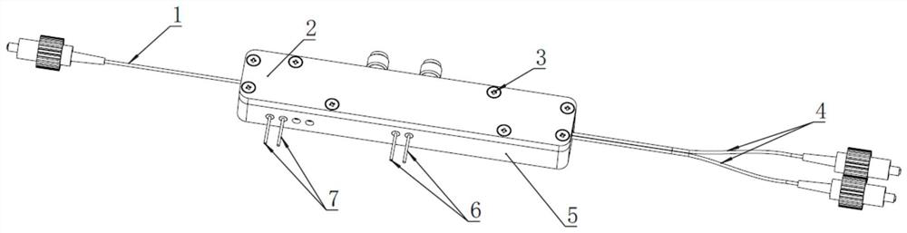
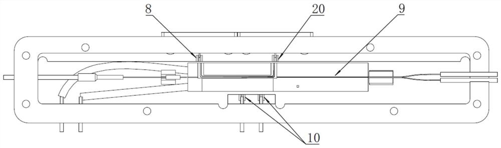
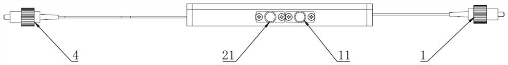
[0048] see figure 1 , figure 2 , a high-speed optical waveguide switch chip packaging module in many embodiments of the present invention, including a metallized optical fiber 1, an upper cover 2, a mounting screw 3, an optical fiber array with a double-ended connector 4, a base 5, a monitoring through-core capacitor 6, Power supply feedthrough capacitor 7, first radio frequency connection ceramic substrate 8, optical waveguide chip 9, monitoring feedthrough capacitor connection ceramic substrate 10, first SMA radio frequency connector 11, fi...


PUM


Abstract

The invention discloses a high-speed optical waveguide switch chip packaging module, and belongs to the field of optical packaging and radio frequency connection integrated modules. The optical waveguide chip comprises a light inlet waveguide, two light outlet waveguides, two grounding electrode plating layers and a radio frequency electrode plating layer; the first end of the metalized optical fiber penetrates into the accommodating cavity through the first end of the base and is coupled with the light inlet waveguide; the optical fiber array with the double-end connector comprises two bare optical fibers; the first radio frequency connection ceramic substrate comprises a first gold-plated layer, a second gold-plated layer and a third gold-plated layer positioned between the first gold-plated layer and the second gold-plated layer; the first SMA radio frequency connector is mounted outside the base; the second radio frequency connection ceramic substrate comprises a fourth gold-plated layer, a fifth gold-plated layer and a sixth gold-plated layer located between the fourth gold-plated layer and the fifth gold-plated layer; and the second SMA radio frequency connector is arranged outside the base. The structure is simple, and optical signals can be conveniently and directly input and output to the module.

Description

technical field [0001] The invention relates to the field of optical packaging and radio frequency connection integrated modules in optical fiber data communication and telecommunication, and mainly relates to a high-speed optical waveguide switch chip packaging module. Background technique [0002] The application of the optical switch module is an indispensable and important part in the optical fiber communication system. At present, the optical switch module generally refers to the function of realizing optical path conversion through an optical waveguide chip, a lens, an optical groove, and the like. Optical switches are generally divided into two categories: mechanical and non-mechanical. One of the non-mechanical types is the optical waveguide switch, which mainly changes the refractive index or other properties of the waveguide through the electro-optic effect, magneto-optic effect, acousto-optic effect, and thermo-optic effect, so that the optical path changes and t...

Claims


Application Information

Patent Timeline
IPC IPC(8): G02B6/35G02B6/02G02B6/04G02B6/42G02B6/26H01R13/02
CPCG02B6/355G02B6/021G02B6/04G02B6/4268G02B6/26G02B6/4201G02B6/4251G02B6/4256H01R13/02
Inventor 李庭军胡荣平何迟光
Owner 上海三菲半导体有限公司
Why Eureka
Try Eureka