
LED epitaxial structure and preparation method thereof

A technology of epitaxial structure and structural layer, which is applied in the direction of semiconductor devices, electrical components, circuits, etc., can solve the problems of high stress in LED epitaxial structure, low LED luminous efficiency, and low lattice quality, so as to improve electron blocking rate and electron utilization rate, lower dislocation density, and larger bandgap

Active Publication Date: 2022-05-27
JUCAN PHOTOELECTRIC TECH (SUQIAN) CO LTD
View PDF5 Cites 0 Cited by
  • Summary
  • Abstract
  • Description
  • Claims
  • Application Information

AI Technical Summary

Problems solved by technology

In order to solve the problems of high stress, high dislocation density and low lattice quality of the existing LED epitaxial structure, which lead to low LED luminous efficiency

Method used


Image

  • LED epitaxial structure and preparation method thereof
  • LED epitaxial structure and preparation method thereof
  • LED epitaxial structure and preparation method thereof

Examples


Embodiment Construction

[0026] Embodiments will be described in detail below, examples of which are illustrated in the accompanying drawings. Where the following description refers to the drawings, the same numerals in different drawings refer to the same or similar elements unless otherwise indicated. The implementations described in the following examples are not intended to represent all implementations consistent with this application. are merely exemplary of systems and methods consistent with some aspects of the present application as recited in the claims.

[0027] LED is a semiconductor light-emitting device that converts electrical energy into light. Compared with traditional light sources, LEDs have the advantages of smaller size, longer service life, lower power consumption and higher response speed. With the wide application of LEDs in the field of lighting, people have higher and higher requirements for the luminous efficiency of LEDs.

[0028] In the existing related art, the method ...


PUM

PropertyMeasurementUnit
Thicknessaaaaaaaaaa
Thicknessaaaaaaaaaa
Thicknessaaaaaaaaaa

Abstract

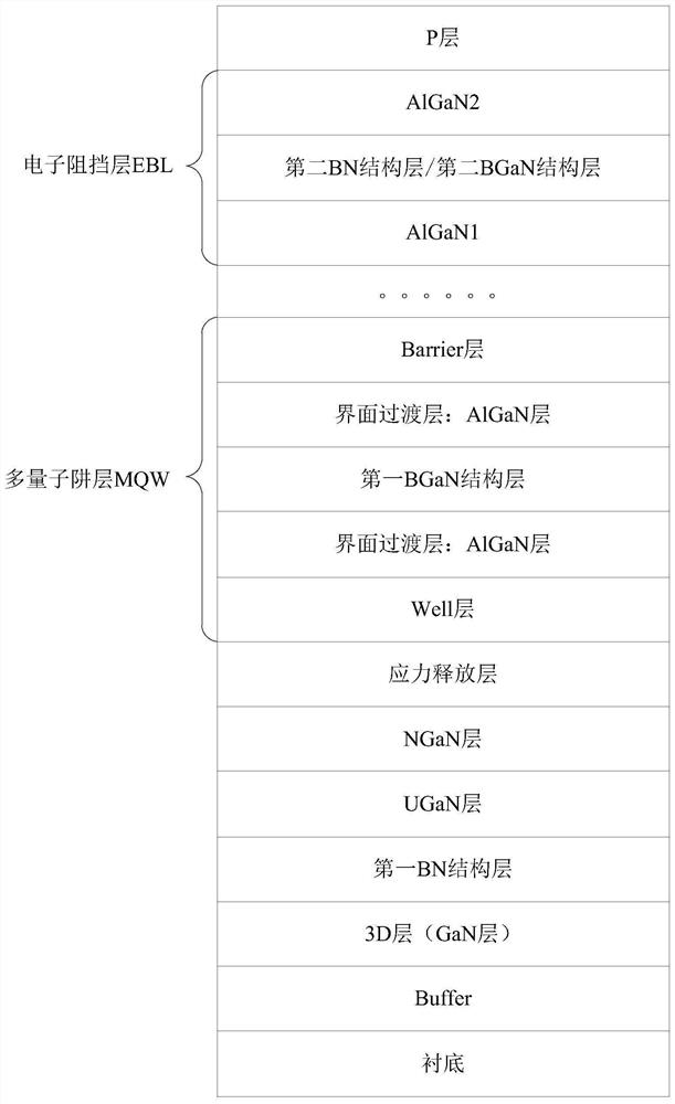
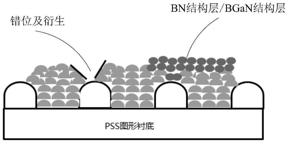
The invention provides an LED epitaxial structure and a preparation method thereof. The LED epitaxial structure comprises a 3D layer, a UGaN layer, a multi-quantum well layer MQW and an electron blocking layer EBL, wherein the multi-quantum well layer MQW comprises an interface transition layer; wherein a first BN structure layer is arranged between the 3D layer and the UGaN layer, a first BGaN structure layer is arranged in the interface transition layer, and a second BN structure layer or a second BGaN structure layer is arranged in the electron blocking layer EBL. According to the invention, the BN structure layer and the BGaN structure layer are inserted into the LED epitaxial structure, and the characteristics of small inter-atomic acting force and large forbidden band width are utilized, so that the dislocation density can be effectively reduced, the stress can be released, and the lattice quality can be improved; and the electron blocking rate and the electron utilization rate are improved, so that the luminous efficiency of the LED is improved.

Description

technical field [0001] The present application relates to the technical field of light-emitting diode (Light-emitting diode, LED) epitaxial growth, and in particular, to an LED epitaxial structure and a preparation method thereof. Background technique [0002] LED is a semiconductor light-emitting device that converts electrical energy into light. Compared with traditional light sources, LEDs have the advantages of smaller size, longer service life, lower power consumption and higher response speed. With the wide application of LEDs in the field of lighting, people have higher and higher requirements for the luminous efficiency of LEDs. [0003] In the existing related technologies, the methods for improving the luminous efficiency of LEDs mainly include: increasing the potential energy difference of the barrier wells in the LEDs, so that more electrons are bound in the well layers, thereby improving the utilization rate of electrons and improving the luminous efficiency; ...

Claims


Application Information

Patent Timeline
IPC IPC(8): H01L33/02H01L33/06H01L33/14H01L33/32H01L33/00
CPCH01L33/025H01L33/06H01L33/145H01L33/32H01L33/0075Y02P70/50
Inventor 徐洋洋江汉徐志军黎国昌程虎王文君苑树伟
Owner JUCAN PHOTOELECTRIC TECH (SUQIAN) CO LTD
Learn More