Heat treatment device

A heat treatment device and heat treatment technology are applied in vacuum evaporation plating, coating, gaseous chemical plating and other directions, which can solve problems such as danger and achieve the effect of reducing installation space.

Pending Publication Date: 2022-06-07
DAINIPPON SCREEN MTG CO LTD
View PDF2 Cites 0 Cited by
  • Summary
  • Abstract
  • Description
  • Claims
  • Application Information

AI Technical Summary

Problems solved by technology

Therefore, when oxidation treatment and nitriding treatment are performed continuously, it is very dangerous to mix ammonia gas which is a combustible gas and oxygen gas which is a combustible gas in the device.

Method used


Image

  • Heat treatment device
  • Heat treatment device
  • Heat treatment device

Examples


Embodiment Construction

[0030] Hereinafter, embodiments of the present invention will be described in detail with reference to the accompanying drawings.

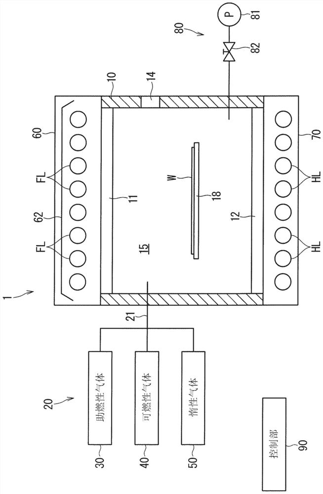
[0031] figure 1 It is a figure which shows the structure of the main part of the heat processing apparatus 1 of this invention. figure 1 The heat treatment apparatus 1 is a flash lamp annealing apparatus, and heats the semiconductor wafer W by irradiating a flash light to the semiconductor wafer W in the shape of a disk as a substrate. The size of the semiconductor wafer W to be processed is not particularly limited, but is, for example, φ300 mm or φ450 mm. also, figure 1 In the drawings and the following figures, the size or number of each part is exaggerated or simplified as necessary for easy understanding.

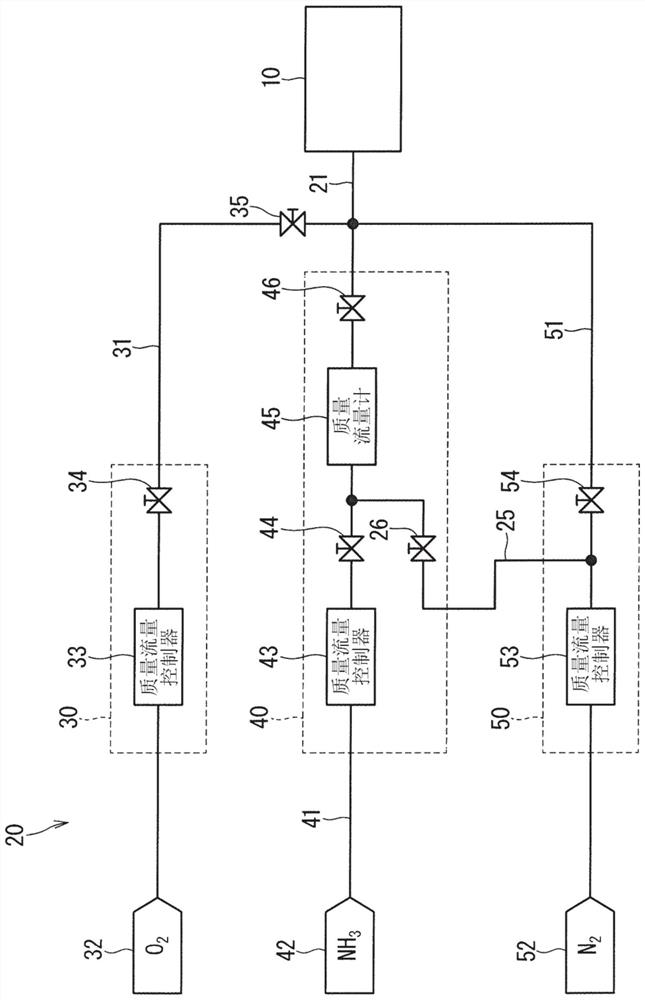
[0032] The heat treatment apparatus 1 includes: a chamber 10 that houses the semiconductor wafers W; a flash irradiation unit 60 that irradiates a flash light to the semiconductor wafers W in the chamber 10 ; a halogen irradiation unit ...


PUM


Abstract

The invention provides a heat treatment device capable of reducing installation space of gas supply related elements. In this heat treatment apparatus, a combustion-supporting gas line (31), a combustible gas line (41), and an inert gas line (51) are connected to a chamber (10) in which a semiconductor wafer is heat-treated. Before the combustible gas is supplied to the chamber (10), nitrogen gas is fed from the inert gas line (51) to the combustion-supporting gas line (31), and the inside of the combustion-supporting gas line (31) is replaced with nitrogen gas. Before the combustion-supporting gas is supplied to the chamber (10), nitrogen gas is fed from the inert gas line (51) to the combustible gas line (41), and the inside of the combustible gas line (41) is replaced with nitrogen gas. The combustion-supporting gas line (31) and the combustible gas line (41) are provided with one common inert gas line (51), so that the installation space of gas supply-related elements can be reduced.

Description

technical field [0001] The present invention relates to a heat treatment device for heating thin-plate precision electronic substrates such as semiconductor wafers (hereinafter simply referred to as "substrates") in a combustible gas or a combustion-supporting gas atmosphere. Background technique [0002] As an apparatus for manufacturing a semiconductor device, a heat treatment apparatus that irradiates a semiconductor wafer with light and heats the semiconductor wafer is widely used. This heat treatment apparatus performs heat treatment of semiconductor wafers in various gas atmospheres. For example, a process of nitriding a semiconductor wafer on which a high dielectric constant film (High-k film) is formed is performed by light irradiation and heating in an ammonia gas atmosphere. In addition, a process of forming an oxide film by heating the silicon semiconductor wafer with light in an oxygen atmosphere is also performed. Furthermore, oxidation treatment may be carrie...

Claims


Application Information

Patent Timeline
Patent Type & Authority Applications(China)
IPC IPC(8): H01L21/67
CPCH01L21/67109H01L21/67017H01L21/67253C23C16/45561C23C16/4408C23C16/46C23C16/482C23C16/345C23C16/402H01L21/67115C23C14/541C23C14/50C23C14/24
Inventor 近藤泰章大森麻央
Owner DAINIPPON SCREEN MTG CO LTD
Why Eureka
Try Eureka