A multi-stage sic-mosfet drive circuit and control method

A drive circuit, multi-stage technology, applied in circuits, electronic switches, electrical components, etc., can solve the problem that the drive circuit drives SiC-based power devices, and cannot take into account the switching delay time of SiC-MOSFET, switching loss current or voltage spikes, device Characteristics difference and other problems, to achieve the effect of optimizing waveform, stabilizing driving voltage, and reducing voltage oscillation

Active Publication Date: 2022-08-05
合肥安赛思半导体有限公司
View PDF8 Cites 0 Cited by
  • Summary
  • Abstract
  • Description
  • Claims
  • Application Information

AI Technical Summary

Problems solved by technology

Compared with Si devices, SiC devices are different in materials and structures, and there are also some differences in device characteristics. Therefore, the existing Si-based power device drive circuits cannot be used to directly drive SiC-based power devices. The latter The drive circuit needs to be specially designed
[0005] In practical applications, the simplest and most common way to adjust the switching characteristics of SiC-MOSFET is to add passive devices in the driving circuit to achieve passive driving. The passive driving circuit has the largest The advantage lies in its simple structure and low cost, but there are also many disadvantages, such as the inability to take into account the SiC-MOSFET switching delay time, switching loss, current or voltage spikes and EMI

Method used


Image

  • A multi-stage sic-mosfet drive circuit and control method
  • A multi-stage sic-mosfet drive circuit and control method
  • A multi-stage sic-mosfet drive circuit and control method

Examples


Embodiment Construction

[0032] A preferred embodiment of the present invention is described in detail below with reference to the accompanying drawings, and many specific details are set forth in the following description to facilitate a full understanding of the present invention. However, the present invention can be implemented in many other ways different from those described herein, and those skilled in the art can make similar improvements without departing from the connotation of the present invention. Therefore, the present invention is not limited by the specific implementation disclosed below.

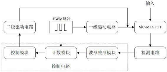
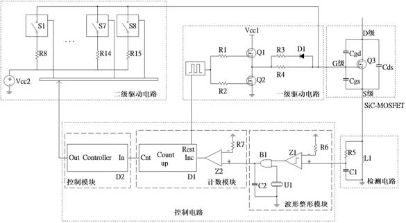
[0033] like figure 1 As shown, the multi-stage SiC-MOSFET drive circuit includes a SiC-MOSFET, a first-stage drive circuit that provides a drive current to turn on the SiC-MOSFET to work, a detection circuit for collecting the voltage dynamic waveform during the turn-on process of the SIC-MOSFET, and a supplementary A secondary drive circuit for driving current and a control circuit for the secondar...


PUM


Abstract

The invention provides a multi-level SiC-MOSFET driving circuit and a control method, including a SiC-MOSFET, a first-level driving circuit for providing a driving current to turn on the SiC-MOSFET, and a voltage dynamic waveform for collecting the voltage dynamic waveform during the turning-on process of the SIC-MOSFET The detection circuit, the secondary driving circuit for supplementing the driving current, and the control circuit for the secondary driving circuit; the control circuit comprises a waveform shaping module, a counting module and a control module which are sequentially signal-connected; the control circuit comprises waveforms which are sequentially signal-connected Shaping module, counting module and control module. The invention realizes the rapid turn-on of the SiC-MOSFET through the two-stage driving circuit, eliminates the voltage peak when turning on, and reduces the voltage oscillation when turning off; and obtains the voltage dynamic parameters during the turning-on process, and then adjusts the secondary driving circuit through the control module to supplement the The size of the drive current to provide a stable drive voltage.

Description

technical field [0001] The invention relates to the technical field of driving of the third-generation wide-bandgap semiconductor silicon carbide device, in particular to a multi-level SiC-MOSFET driving circuit and a control method. Background technique [0002] One of the future development trends of the power electronics industry is to use higher switching frequencies to achieve tighter system design. In applications with high switching frequencies and high power, SiC devices have obvious advantages, which makes SiC-MOSFETs suitable for 5G base stations. , industrial power supply, photovoltaics, charging piles, uninterruptible power supply systems, and energy storage and other application scenarios are constantly increasing. [0003] SiC (Silicon Carbide) is a third-generation semiconductor. Compared with similar products, SiC has significant advantages in key parameters such as forbidden band width, breakdown electric field strength, saturated electron drift rate, therma...

Claims


Application Information

Patent Timeline
Patent Type & Authority Patents(China)
IPC IPC(8): H03K17/041H03K17/16H03K17/687
CPCH03K17/04106H03K17/161H03K17/687
Inventor 曹文平胡存刚孙路严志尚朱非凡
Owner 合肥安赛思半导体有限公司
Why Eureka
Try Eureka