
Fan-out packaging structure and fan-out packaging method

A packaging structure, fan-out technology, applied in the direction of semiconductor/solid-state device components, semiconductor devices, electrical components, etc., can solve the problems of increasing the parasitic effect of the circuit layer and the capacitance effect, the number of conductive holes, and the complex wiring layer process. , to reduce parasitic effects and capacitance effects, simplify process steps, and improve heat dissipation effects

Active Publication Date: 2022-06-21
FOREHOPE ELECTRONICS NINGBO CO LTD
View PDF11 Cites 1 Cited by
  • Summary
  • Abstract
  • Description
  • Claims
  • Application Information

AI Technical Summary

Problems solved by technology

When the number of rewiring layers produced is more, the required wiring layer process is more complicated, and the number of conductive holes will be more, resulting in an increase in cost
In addition, the conductive holes on the rewiring layer will inevitably increase the parasitic effect and capacitance effect between the wiring layers, which will cause signal transmission to be interfered and the heat dissipation effect of the product will be poor.

Method used


Image

  • Fan-out packaging structure and fan-out packaging method
  • Fan-out packaging structure and fan-out packaging method
  • Fan-out packaging structure and fan-out packaging method

Examples


no. 1 example

[0083] To sum up, the fan-out packaging structure 100 and method provided by the embodiments of the present invention have the following beneficial effects:

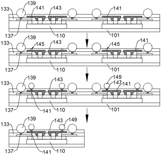
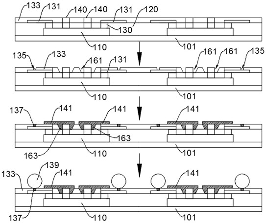
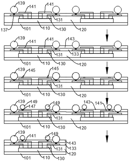
[0084] In the fan-out packaging method provided by the embodiment of the present invention, the first pad 130 and the second pad 140 with different heights are formed on the chip 110, and the first wiring layer is drawn out from the first pad 130 and the second pad 140 respectively. 131 and the second wiring layer 141 can simplify the process without additionally setting conductive holes and conductive columns, while reducing parasitic effects and capacitive effects, avoiding signal transmission interference, and improving product heat dissipation.

[0085] The above is only a specific embodiment of the present invention, but the scope of protection of the present invention is not limited thereto. Anyone skilled in the art can easily think of changes or substitutions within the technical scope disclosed in the present inv...

no. 2 example


PUM


Abstract

The invention provides a fan-out type packaging structure and a fan-out type packaging method, and relates to the technical field of semiconductors. The structure comprises a packaging element, a plastic packaging body, a first dielectric layer and a second dielectric layer, the packaging element is provided with a first bonding pad and a second bonding pad, the first bonding pad is lower than the second bonding pad, the plastic packaging body packages the packaging element in a plastic mode, the end face of the first bonding pad is exposed out of the surface of the plastic packaging body, and the end face of the second bonding pad is exposed out of the surface of the plastic packaging body. A first wiring layer is arranged on one side, far away from the packaging element, of the first bonding pad, and a first welding ball is arranged on the first wiring layer; the first dielectric layer is arranged on the side, away from the packaging element, of the first wiring layer, the end face of the second bonding pad is exposed out of the surface of the first dielectric layer, a second wiring layer is arranged on the side, away from the packaging element, of the second bonding pad, and second welding balls are arranged on the second wiring layer; a second dielectric layer is arranged on the side, away from the first wiring layer, of the second wiring layer. The structure can reduce the number of wiring layers and does not need to additionally increase conductive columns.

Description

technical field [0001] The present invention relates to the technical field of semiconductors, in particular to a fan-out packaging structure and a fan-out packaging method. Background technique [0002] In the existing fan-out process, it is usually necessary to arrange multiple layers of rewiring layers to connect the functional pads and ground pads on the chip to the outside. However, connecting the ground pads or functional pads to the outside requires conductive vias. , The conductive pillar connects the multi-layer rewiring layer to realize the fan-out expansion of the chip pad. When the number of rewiring layers produced is more, the required wiring layer process is more complicated, and the number of conductive holes will be more, resulting in an increase in cost. In addition, the conductive holes on the rewiring layer will inevitably increase the parasitic effect and capacitive effect between the wiring layers, which will cause signal transmission to be interfered ...

Claims


Application Information

Patent Timeline
IPC IPC(8): H01L23/485H01L21/60
CPCH01L23/4824H01L23/485H01L24/03H01L2224/0231H01L2224/02331H01L2224/02333H01L2224/02379H01L2224/02381H01L2224/18H01L21/6723H01L2221/68345H01L21/568H01L21/6835H01L21/561H01L24/96H01L23/562H01L21/4853H01L23/3128H01L23/49816H01L23/49838
Inventor 高源胡彪
Owner FOREHOPE ELECTRONICS NINGBO CO LTD
Learn More