Packaging structure of photoelectric module and photoelectric module using packaging structure

A technology for optoelectronic modules and packaging structures, applied in the field of optical communication, can solve the problems of many structural parts and complex assembly, and achieve the effects of simple structure, flexible structure and avoidance of damage.

Active Publication Date: 2022-06-24
EVERPRO TECH COMPANY
View PDF5 Cites 0 Cited by
  • Summary
  • Abstract
  • Description
  • Claims
  • Application Information

AI Technical Summary

Problems solved by technology

However, in this type of transceiver integrated optical module, the optical transceiver device and the printed circuit board are installed in the base, and the optical transceiver device needs a fixed position provided by the base, otherwise the coupling and alignment with the optical fiber cannot be completed.
This structure has many parts and complex assembly

Method used


Image

  • Packaging structure of photoelectric module and photoelectric module using packaging structure
  • Packaging structure of photoelectric module and photoelectric module using packaging structure
  • Packaging structure of photoelectric module and photoelectric module using packaging structure

Examples


Embodiment 1

[0061] see Figure 4 , Figure 5 , showing an embodiment of an optical assembly according to the present invention.

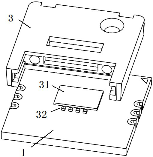
[0062] In this embodiment, the optical assembly 3 includes a first lens 33, a second lens 35 and a reflection device 34, the optical assembly 3 has an accommodating inner cavity, the first lens is connected to the light emitting / receiving device The optical window of the device 32 is aligned and attached to the substrate. The reflecting device 34 is used to couple the optical path of the first lens 33 and the optical path of the second lens 35, and the second lens 35 and the optical fiber 8's cutouts are aligned for installation.

[0063] Specifically, the first lens 33 can be a horizontal lens, the reflective device 34 can be a 45-degree oblique reflective surface, the second lens 35 can be a vertical lens, and the horizontal lens is used to align the light window of the light emitting / receiving device 32 and attached to the substrate 1 , the reflective sur...

Embodiment 2

[0068] see Image 6 , showing another embodiment of an optical assembly according to the present invention, the optical path coupling between the light emitting / receiving device and the optical fiber can also be realized by means of the optical fiber guide hole.

[0069] The optical component is an optical fiber guide hole 6 , the light emitting / receiving device 32 is installed on the bracket 4 , the bracket 4 is installed on the substrate 1 , and the optical fiber guiding hole 6 is aligned with the light of the light emitting / receiving device 31 . the center of the window, so as to realize the optical coupling between the optical fiber and the light transmitting / receiving device.

[0070] In this embodiment, the front and side surfaces of the bracket 4 can be provided with conductive lines. After the bracket 4 is rotated by 90 degrees, it is installed on the substrate 1. The optical fiber guide hole 6 is installed on the side frame 5, and the optical fiber guides The hole 6 ...


PUM


Abstract

The invention discloses a packaging structure of a photoelectric module and the photoelectric module using the packaging structure, the packaging structure comprises a centrosymmetric substrate, one surface of the substrate is provided with a plurality of light emitting / receiving devices and a driver, and the other surface of the substrate is provided with a plurality of electrical contacts; the electrical contacts comprise a plurality of first contacts and a plurality of second contacts, the second contacts are arranged on the peripheries of the first contacts, intervals are arranged between the second contacts, and the surface area of the first contacts is larger than that of the second contacts. The photoelectric module can be suitable for different types of optical assemblies. According to the invention, the base is directly used for installing the light emitting / receiving device, and the assembly process is simple; a plurality of electrical contacts are arranged on the back surface of the substrate and are suitable for a reflow soldering surface mounting process; the optical assembly is protected through the protective cover, injection molding materials can be prevented from entering the inner cavity, and the device is suitable for different modes and is flexible and simple in structure.

Description

technical field [0001] The invention relates to the field of optical communication, in particular, to a packaging structure of an optoelectronic module and an optoelectronic module using the packaging structure, which simplifies the assembly process. Background technique [0002] As the density and integration of communication electronic devices increase, optical transceiver modules are required to have smaller size packages. [0003] The common method in the industry is to encapsulate the chip in the secondary PCBA, connect the secondary PCBA to the optical fiber connector, and then assemble them together on the main PCB. The secondary PCB has certain versatility. Although this structure omits the conversion of the lens optical path, it limits the optical coupling between the secondary PCBA and the fiber optic connector to use only active coupling, which requires longer coupling time than passive coupling, and is more efficient in production. Low. And the main PCBA and t...

Claims


Application Information

Patent Timeline
Patent Type & Authority Applications(China)
IPC IPC(8): G02B6/42
CPCG02B6/4287G02B6/4237G02B6/4206G02B6/4214G02B6/428
Inventor 王群泽周一环江辉汪绪茂
Owner EVERPRO TECH COMPANY
Why Eureka
Try Eureka