Metal oxide thin film transistor, manufacturing method thereof and array substrate

A technology of oxide thin film and manufacturing method, which is applied in the direction of transistors, semiconductor/solid-state device manufacturing, semiconductor devices, etc., can solve the problems of complicated process and difficult to obtain driving performance of metal oxide thin film transistors, etc., and achieve simple manufacturing process and excellent driving performance Effect

Pending Publication Date: 2022-06-28
KUSN INFOVISION OPTOELECTRONICS
View PDF0 Cites 0 Cited by
  • Summary
  • Abstract
  • Description
  • Claims
  • Application Information

AI Technical Summary

Problems solved by technology

The formation of the above metal oxide thin film transistors requires at least five layers of film-forming processes, and at least two layers of different materials must be deposited in the gate insulating layer 3. The whole process is relatively complicated, and it is difficult to obtain metal oxide thin film transistors with excellent driving performance.

Method used


Image

  • Metal oxide thin film transistor, manufacturing method thereof and array substrate
  • Metal oxide thin film transistor, manufacturing method thereof and array substrate
  • Metal oxide thin film transistor, manufacturing method thereof and array substrate

Examples


Embodiment Construction

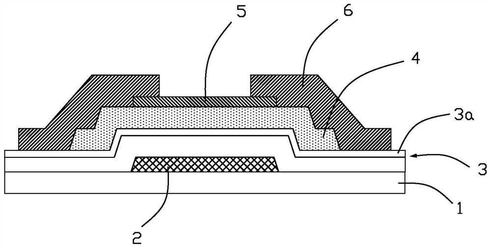
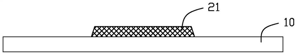
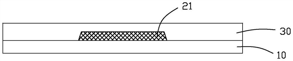
[0022] In order to further illustrate the technical means and effects adopted by the present invention to achieve the predetermined purpose of the invention, the following describes the specific implementation of the metal oxide thin film transistor, its manufacturing method and the array substrate according to the present invention with reference to the accompanying drawings and preferred embodiments. The methods, structures, features and their effects are described in detail as follows:

[0023] The foregoing and other technical contents, features and effects of the present invention will be clearly presented in the following detailed description of the preferred embodiments with reference to the drawings. Through the description of the specific embodiments, the technical means and effects adopted by the present invention to achieve the predetermined purpose can be more deeply and specifically understood. However, the accompanying drawings are only used for reference and desc...


PUM


Abstract

The invention provides a metal oxide thin film transistor which comprises a substrate, a grid electrode, a grid electrode insulating layer, a titanium oxide layer, a source electrode, a drain electrode and a metal oxide semiconductor layer. The titanium oxide layer is formed on the gate insulating layer; a source electrode and a drain electrode are formed on the gate insulating layer, the source electrode comprises a source electrode bottom layer and a source electrode top layer which have the same pattern, and the drain electrode comprises a drain electrode bottom layer and a drain electrode top layer which have the same pattern. The source electrode bottom layer and the drain electrode bottom layer are made of titanium, and the source electrode bottom layer, the drain electrode bottom layer and the titanium oxide layer are formed on the same layer. The metal oxide semiconductor layer is formed on the source top layer and the drain top layer, and the metal oxide semiconductor layer is located between the source top layer and the drain top layer and covers part of the source top layer, part of the drain top layer and the titanium oxide layer located between the source top layer and the drain top layer. The metal oxide thin film transistor is simple in manufacturing process and excellent in driving performance. The invention further relates to a manufacturing method of the metal oxide thin film transistor and an array substrate.

Description

technical field [0001] The present invention relates to the field of display technology, in particular to a metal oxide thin film transistor, a manufacturing method thereof, and an array substrate. Background technique [0002] In recent years, Oxide Semiconductor Thin Film Transistor (AOS TFT) has received extensive attention in the industry due to its good electrical and optical properties. However, thin film transistors using metal oxide semiconductors as active layer materials are usually formed by sputtering, atomic layer deposition (ALD), pulsed laser deposition (PLD), metal organic chemical vapor deposition (MOCVD), etc. Vapor deposition methods, or liquid deposition methods such as solution coating, ink jet printing, etc., the metal oxide semiconductor films deposited by any of the foregoing deposition methods contain a large number of microscopic structural defects, such as micropores (void), vacancy (vacancy), dislocation, chemical bond length / bond angle strain (s...

Claims


Application Information

Patent Timeline
IPC IPC(8): H01L29/786H01L29/417H01L21/34
CPCH01L29/66969H01L29/78693H01L29/41733
Inventor 陈晓威
Owner KUSN INFOVISION OPTOELECTRONICS
Why Eureka
Try Eureka