

Semiconductor structure and preparation method thereof
A semiconductor and gate structure technology, which is applied in semiconductor/solid-state device manufacturing, semiconductor devices, semiconductor/solid-state device components, etc., can solve problems such as expensive pattern forming equipment, achieve short-channel effect suppression, and avoid threshold voltage drift , Improve the effect of integration and performance
- Summary
- Abstract
- Description
- Claims
- Application Information
AI Technical Summary
Problems solved by technology
Method used
Image

Examples
Embodiment Construction
[0018] The specific embodiments of the semiconductor structure and the preparation method thereof provided by the present disclosure will be described in detail below with reference to the accompanying drawings.
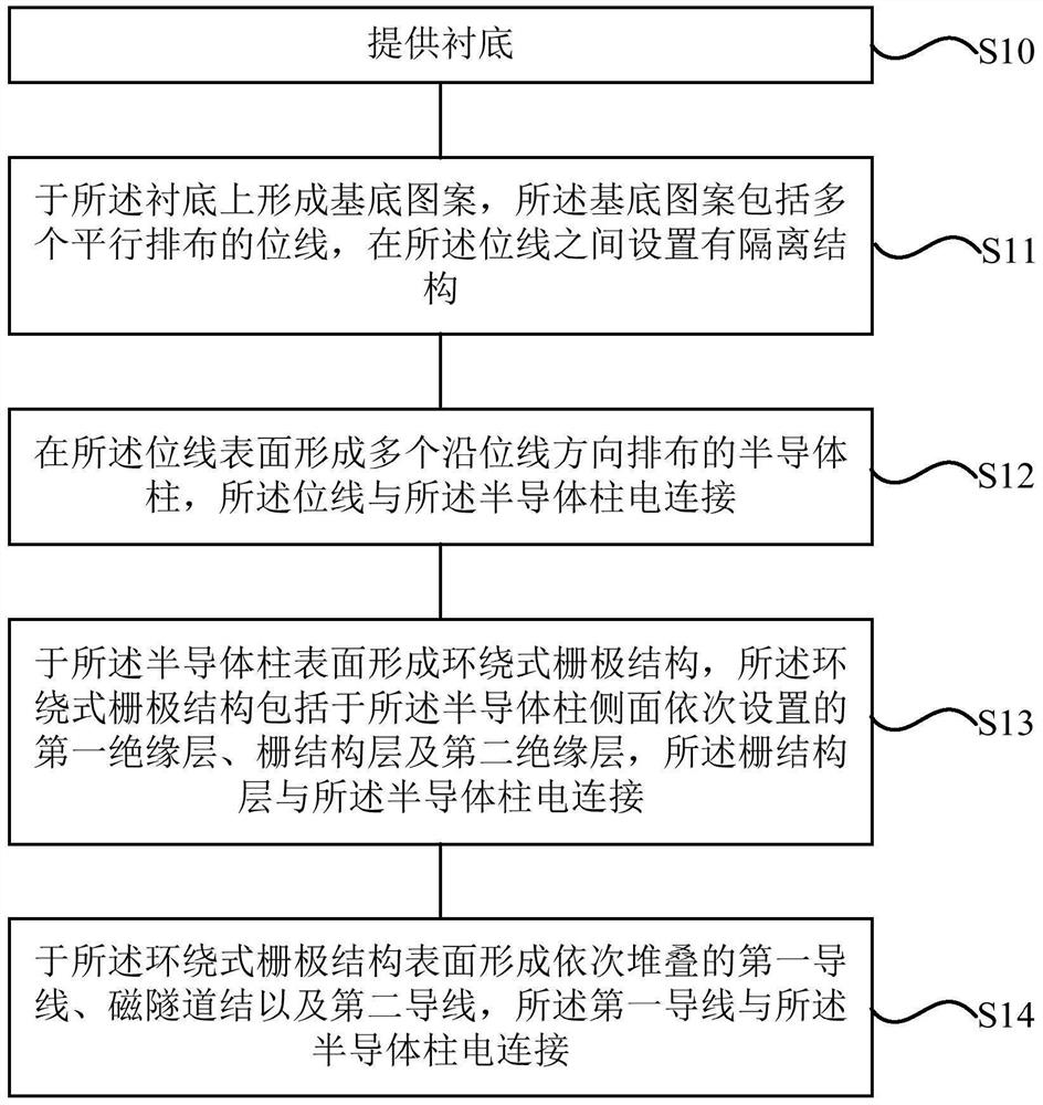
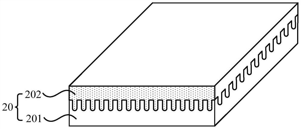
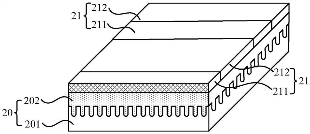
[0019] figure 1 A schematic diagram of steps of a method for fabricating a semiconductor structure provided in an embodiment of the present disclosure. see figure 1 , the semiconductor structure preparation method includes the following steps: step S10, providing a substrate 20; step S11, forming a base pattern 21 on the substrate 20, and the base pattern 21 includes a plurality of bit lines 211 arranged in parallel, An isolation structure 212 is provided between the bit lines; in step S12 , a plurality of semiconductor pillars 22 arranged in the direction of the bit lines are formed on the surface of the bit line table 211 , and the bit lines 211 are electrically connected to the semiconductor pillars 22 . connection; step S13 , forming a wraparound gate structure...
PUM
 Abstract
Description
Claims
Application Information