Preparation method of optical modulator based on glass microstructure array

A glass microstructure and optical modulator technology, applied in glass manufacturing equipment, glass molding, microstructure technology, etc., can solve the problems of long processing time, difficult molding, high cost, etc., to improve light transmission performance and reduce glass- Silicon bonding step, the effect of improving production efficiency

Pending Publication Date: 2022-07-08
INSTR TECH & ECONOMY INST P R CHINA +2
View PDF0 Cites 0 Cited by
  • Summary
  • Abstract
  • Description
  • Claims
  • Application Information

AI Technical Summary

Problems solved by technology

The existing dry etching process is slow and costly. The current glass reflow process is generally realized by anodic bonding and high temperature annealing. There are still problems such as long processing time and difficult molding in the preparation of high aspect ratio glass microstructures.

Method used


Image

  • Preparation method of optical modulator based on glass microstructure array
  • Preparation method of optical modulator based on glass microstructure array
  • Preparation method of optical modulator based on glass microstructure array

Examples


preparation example Construction

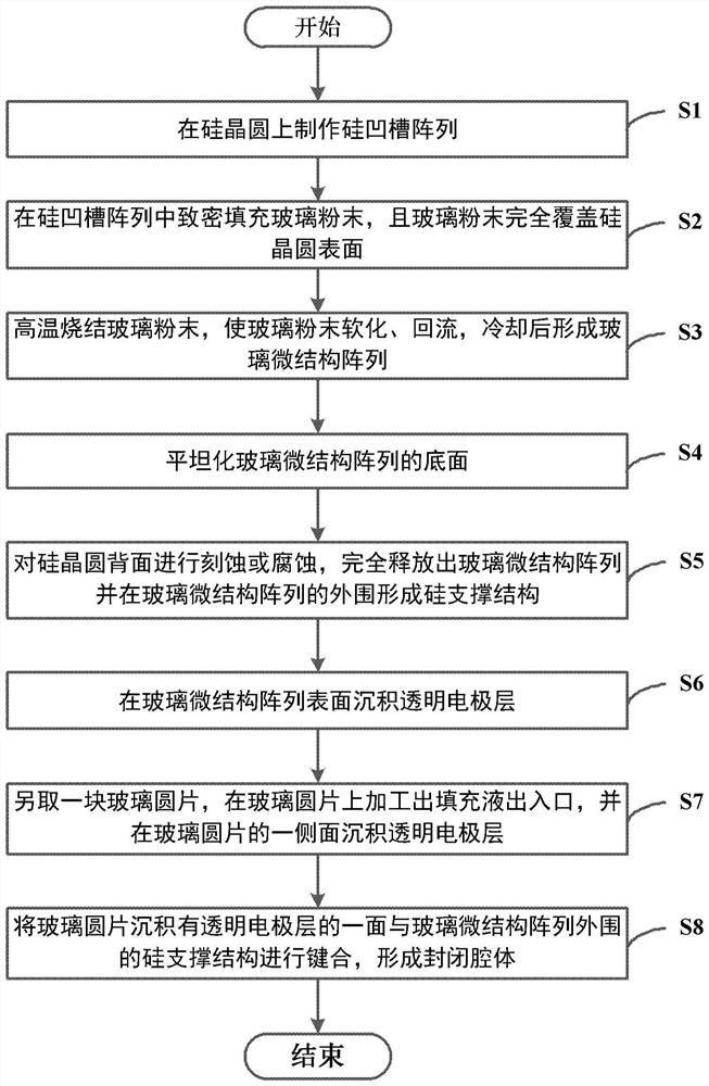
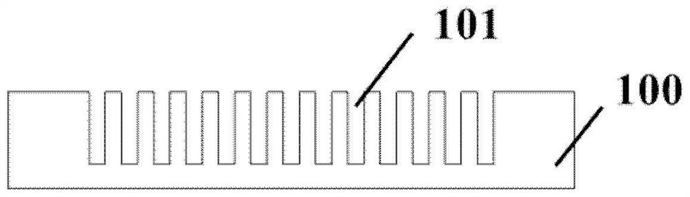
[0046] The preparation method of an optical modulator based on a glass microstructure array provided by the present disclosure utilizes nano-glass powder sintering and thermal reflow molding to realize the preparation of ultra-high depth and width glass microstructures, such as figure 1 As shown, the method includes the following steps:

[0047] Step S1: fabricating a silicon groove array on a silicon wafer;

[0048] Step S2: densely filling the silicon groove array with glass powder, and the glass powder completely covers the surface of the silicon wafer;

[0049] Step S3: sintering the glass powder at a high temperature to soften and reflow the glass powder, and form a glass microstructure array after cooling;

[0050] Step S4: planarizing the bottom surface of the glass microstructure array;

[0051] Step S5: etching or etching the back of the silicon wafer, completely releasing the glass microstructure array, and forming a silicon support structure on the periphery of th...


PUM


Abstract

The invention provides a preparation method of an optical modulator based on a glass microstructure array. The preparation method comprises the following steps: manufacturing a silicon groove array on a silicon wafer; compactly filling glass powder in the silicon groove array; sintering the glass powder at high temperature to soften, reflow and cool the glass powder to form a glass microstructure array; planarizing the bottom surface of the glass microstructure array; etching or corroding the back surface of the silicon wafer to completely release the glass microstructure array, and forming a silicon support structure on the periphery of the glass microstructure array; depositing a transparent electrode layer on the surface of the glass microstructure array; another glass wafer is taken, a filling liquid inlet and a filling liquid outlet are machined in the glass wafer, and a transparent electrode layer is deposited on one side face of the glass wafer; and bonding the surface, on which the transparent electrode layer is deposited, of the glass wafer with the silicon supporting structure on the periphery of the glass microstructure array to form a closed cavity. According to the invention, the glass microstructure array with a high aspect ratio can be obtained, so that the optical modulator is prepared.

Description

technical field [0001] The present disclosure relates to the technical field of manufacturing micro-nano electromechanical systems, and in particular, to a preparation method of an optical modulator based on a glass microstructure array. Background technique [0002] Light field imaging restores the visual information of the three-dimensional world by calculating and processing the collected light field data, making up for the deficiency that traditional imaging can only record two-dimensional information, and is considered to be an important next-generation display imaging technology. [0003] Introducing an optical modulator into a camera is one of the main ways to realize light field acquisition at present. The use of glass microstructure arrays in optical modulators is a beneficial attempt to break the constraints between the light field acquisition angle and spatial resolution and maintain a high signal-to-noise ratio. Among them, the aspect ratio of the glass microstr...

Claims


Application Information

Patent Timeline
IPC IPC(8): B81C1/00C03B19/01C03C17/23C03C27/00
CPCC03B19/01C03C17/23C03C27/00B81C1/00119B81C1/00444C03C2217/231C03C2217/24B81C2201/0102
Inventor 朱敏杰杜晓辉刘帅刘丹熊艳伟李小娟刘瑞
Owner INSTR TECH & ECONOMY INST P R CHINA
Why Eureka
Try Eureka