Self-purification method for reducing Dimple rate in Gringing process

A self-purification, silicon wafer technology, applied in machine tools, manufacturing tools, grinders and other directions suitable for grinding workpiece planes, can solve problems such as increasing the scrap rate of silicon wafers, increasing the overall cost of production and processing, and affecting nanometer topography.

Pending Publication Date: 2022-07-15
中环领先半导体材料有限公司
View PDF0 Cites 0 Cited by
  • Summary
  • Abstract
  • Description
  • Claims
  • Application Information

AI Technical Summary

Problems solved by technology

[0004] The purpose of the present invention is to provide a self-purification method that reduces the Dimple rate of the Grinding process, to solve the problem of Dimple in the existing silicon wafer manufacturing Grinding proposed in the above-mentioned background technology, which seriously affects the nano-morphology, so the Grinding process is reduced. The Dimple rate is very important, and at the same time, the scrap rate of silicon wafers is greatly increased, which increases the overall cost of production and processing.

Method used


Image

  • Self-purification method for reducing Dimple rate in Gringing process
  • Self-purification method for reducing Dimple rate in Gringing process
  • Self-purification method for reducing Dimple rate in Gringing process

Examples


Embodiment 1

[0020] The self-purification method of the present embodiment comprises the following steps:

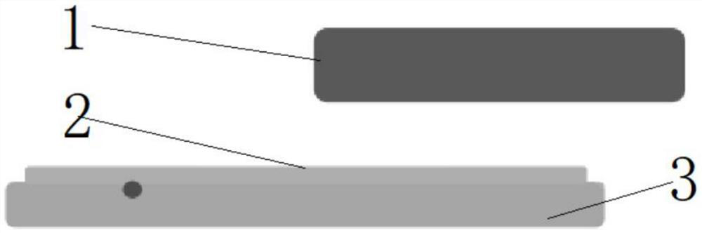
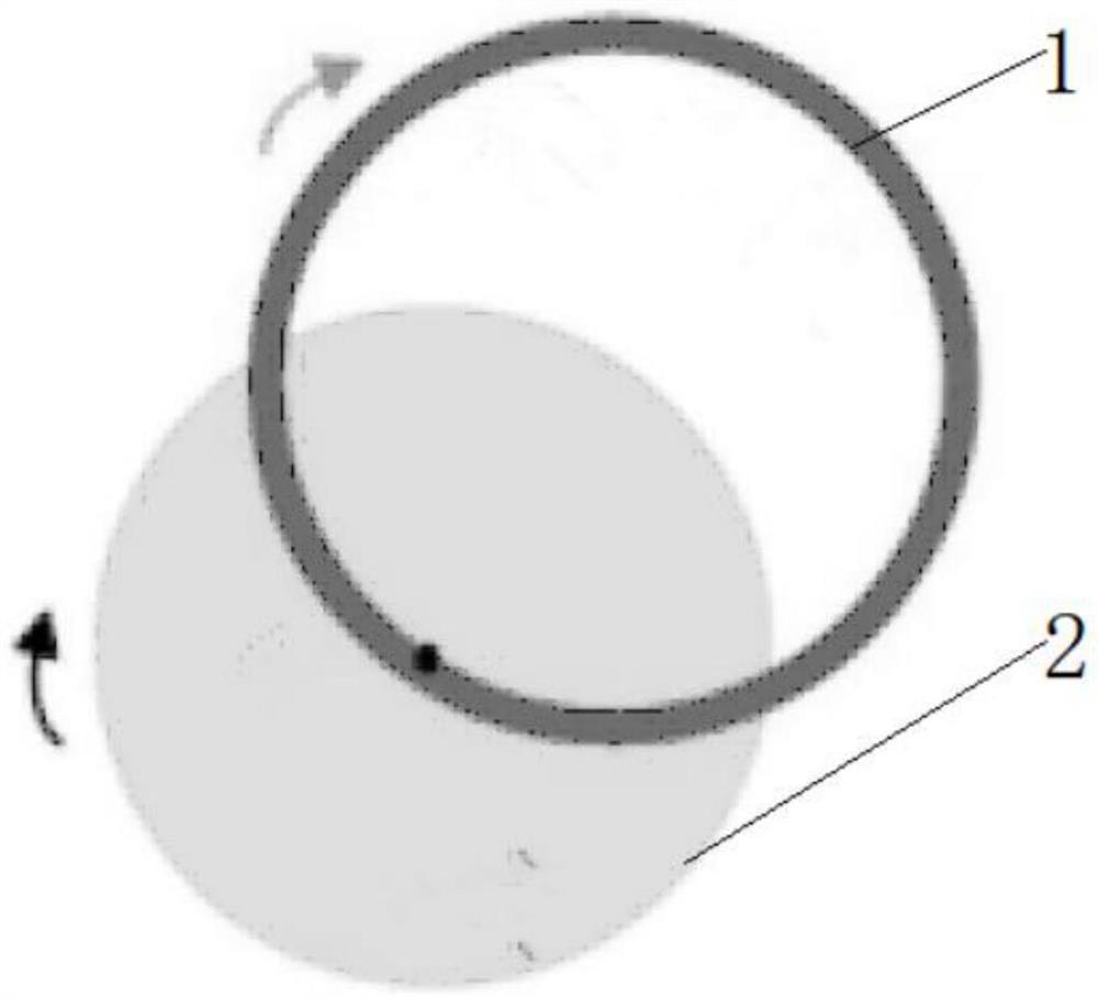
[0021] S1. First, prepare the silicon wafer material to be processed for use, and release the vacuum through the Table to generate suction, adsorb the silicon wafer to be processed on its surface, and use a grinding wheel to grind and purify the silicon wafer from above in real time.

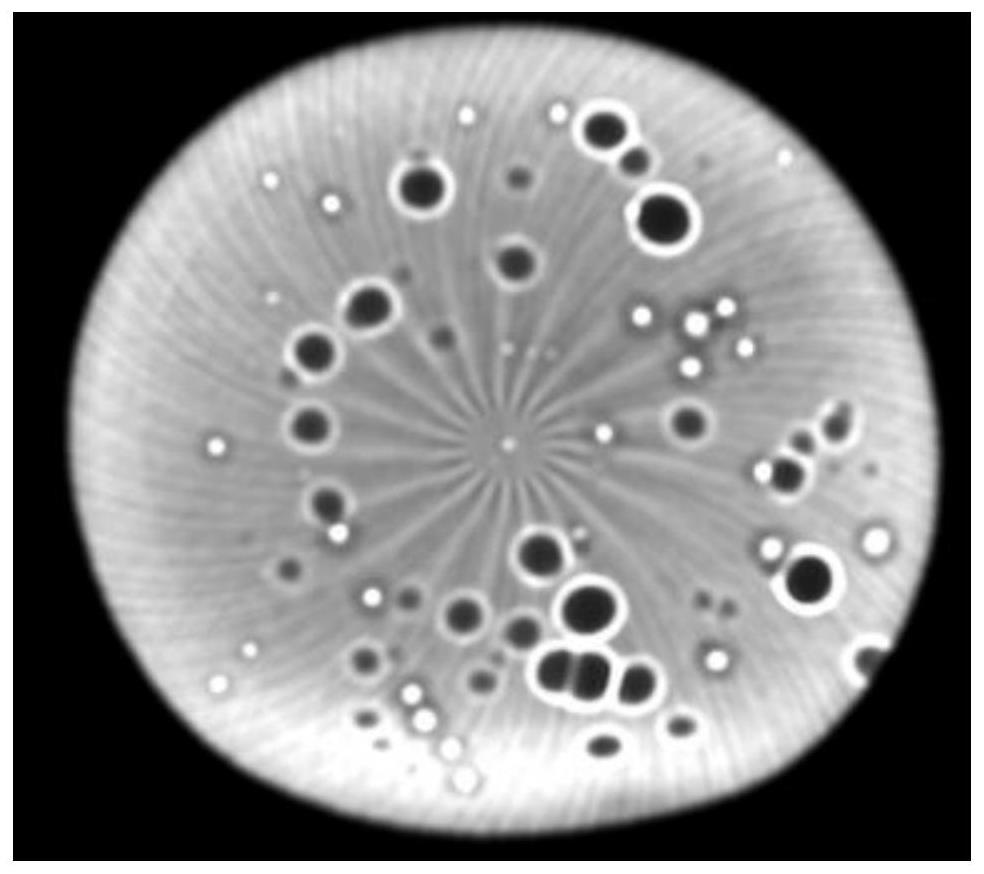
[0022] S2. Then in the process of grinding and purification, according to the actual needs of grinding and purification, personnel can adjust the rotation speed of the table in real time, so that the rotation speed of the table can be adjusted to a minimum, thereby effectively reducing the influence of centrifugal force and avoiding the lack of ceramic holes on the edge. , the edge impurities are not easy to be excluded and the edge Dimple problem has a greater impact on the back pass, which makes the back pass more difficult to repair.

[0023] S3. Finally, increase the air volume in the outer ring of...

Embodiment 2

[0027] The difference with the first embodiment is:

[0028] The self-purification method of the present embodiment comprises the following steps:

[0029] First, prepare the silicon wafer material to be processed for standby, and release the vacuum through the Table to generate suction, adsorb the silicon wafer to be processed on its surface, and use the grinding wheel to grind and purify the silicon wafer from above in real time, and set the grinding wheel to process The process speed is equal to the purification (that is, the non-grinding process) speed, and the speed of the table processing process is set equal to the purification (that is, the non-grinding process) speed, and the air blowing volume and the water blowing flow of each hole of the table ceramic hole are set to be the same. .

[0030] To sum up: the results of the present invention in Example 1 of the present invention show that, compared with the results of the traditional self-cleaning method in Example 2,...


PUM


Abstract

The invention discloses a self-purification method for reducing the Dimple rate in the Gringing process, and the self-purification method comprises the following steps: S1, firstly preparing a silicon wafer material needing to be processed for later use, releasing vacuum through Table to generate suction force, adsorbing the silicon wafer needing to be processed onto the surface of the silicon wafer material, and grinding and purifying the silicon wafer in real time from the upper side by adopting a grinding wheel; and S2, in the grinding and purifying process, the rotating speed of the Table can be adjusted in real time by personnel according to the actual grinding and purifying requirements, so that the rotating speed of the Table is adjusted to be reduced to the minimum, the influence of centrifugal force is effectively reduced, and the problems that the edge is not provided with ceramic holes, edge impurities are not easy to remove, and the edge Dimple has greater influence on the subsequent process are solved. And the subsequent process is difficult to repair. Through the optimization of the purification mode, the Dimple rate in the Gringing process can be greatly reduced in a floating manner, the problem that the Dimple is located on the edge in the Gringing process can be avoided, the silicon wafer is prevented from being scrapped due to poor nanometer morphology, and the product yield is improved.

Description

technical field [0001] The invention relates to the technical field of semiconductor manufacturing, in particular to a self-purification method for reducing the Dimple rate of a Grinding process. Background technique [0002] With the rapid development of the IC industry, the chip size continues to increase, the integrated circuit design line width continues to decrease, and the quality requirements for the interior of the silicon material crystal and the surface of the silicon wafer are getting higher and higher. The requirements for the surface of silicon materials are becoming more and more stringent, and the quality of the surface directly affects the processing quality and yield of the device. The change trend is consistent with the change of the nanometer topography on the surface of the silicon wafer, which is a good indication that the nanometer topography has a very direct impact on the quality of lithography. On a silicon wafer with large rice grains, 160,000 trans...

Claims


Application Information

Patent Timeline
IPC IPC(8): H01L21/304H01L21/67B24B7/22
CPCH01L21/304H01L21/67253B24B7/228
Inventor 刘姣龙蒋文斌李苏峰邓欢武卫刘建伟
Owner 中环领先半导体材料有限公司
Why Eureka
Try Eureka