Manufacturing method of semiconductor power device

A technology for power devices and manufacturing methods, which is applied in semiconductor/solid-state device manufacturing, electrical components, circuits, etc., and can solve problems such as metal falling off on the backside

Pending Publication Date: 2022-07-29
SHANGHAI HUAHONG GRACE SEMICON MFG CORP
View PDF0 Cites 0 Cited by
  • Summary
  • Abstract
  • Description
  • Claims
  • Application Information

AI Technical Summary

Problems solved by technology

[0005] In view of this, the present invention provides a method for manufacturing a semiconductor power devi

Method used


Image

  • Manufacturing method of semiconductor power device
  • Manufacturing method of semiconductor power device
  • Manufacturing method of semiconductor power device

Examples


Embodiment Construction

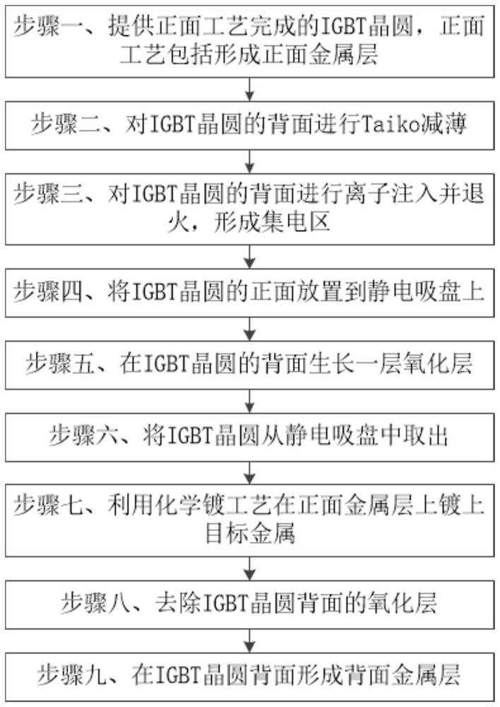
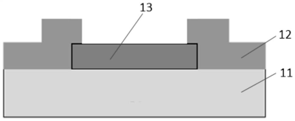
[0034] The present invention is described below based on examples, but the present invention is not limited to these examples only. In the following detailed description of the invention, some specific details are described in detail. The present invention can be fully understood by those skilled in the art without the description of these detailed parts. Well-known methods, procedures, procedures, components and circuits have not been described in detail in order to avoid obscuring the essence of the present invention.

[0035] Furthermore, those of ordinary skill in the art will appreciate that the drawings provided herein are for illustrative purposes and are not necessarily drawn to scale.

[0036] Unless clearly required by the context, words such as "including", "comprising" and the like throughout this application should be construed in an inclusive rather than an exclusive or exhaustive sense; that is, in the sense of "including but not limited to".

[0037] In the d...


PUM

PropertyMeasurementUnit
Thicknessaaaaaaaaaa

Abstract

The invention provides a manufacturing method of a semiconductor power device, and the method comprises the steps: providing an IGBT wafer of which the front process is completed, and the front process comprises the steps: forming a front metal layer; carrying out Taiko thinning on the back surface of the IGBT wafer; performing ion implantation and annealing on the back surface of the IGBT wafer to form a collector region; placing the front surface of the IGBT wafer on an electrostatic chuck; growing an oxide layer on the back surface of the IGBT wafer; taking out the IGBT wafer from the electrostatic chuck; plating target metal on the front metal layer by using a chemical plating process; removing the oxide layer on the back surface of the IGBT wafer; and forming a back metal layer on the back of the IGBT wafer. According to the method, the oxide layer is formed on the back surface of the IGBT wafer before the chemical plating process is carried out, so that the back surface of the wafer is protected by the oxide layer, the problem that metal on the back surface falls off due to the IGBT chemical plating process is solved, and wafer fragments or machine contamination are avoided.

Description

technical field [0001] The present invention relates to the technical field of semiconductor manufacturing, in particular to a method for manufacturing a semiconductor power device. Background technique [0002] IGBT (Insulated Gate Bipolar Transistor, Insulated Gate Bipolar Transistor) is the core device in new energy power electronic products. The evolution of high-end products such as automobiles. [0003] At present, IGBT is developing in the direction of high voltage and high current, and the chip technology and packaging of IGBT are facing new challenges. In order to realize the heat dissipation of the IGBT overall module, the welding process in the package has been developed from the traditional aluminum welding wire to the copper sheet welding, which has higher requirements on the thickness and hardness of the entire front metal of the IGBT. [0004] In order to make the thickness and hardness of the metal on the front side of the IGBT meet the requirements, people...

Claims


Application Information

Patent Timeline
IPC IPC(8): H01L21/56H01L21/288H01L21/331
CPCH01L21/56H01L21/288H01L29/66325
Inventor 潘嘉杨继业姚一平黄璇
Owner SHANGHAI HUAHONG GRACE SEMICON MFG CORP
Why Eureka
Try Eureka