Semiconductor integrated circuit apparatus and fabrication method thereof

Inactive Publication Date: 2005-01-25
FUJITSU LTD
View PDF1 Cites 3 Cited by
  • Summary
  • Abstract
  • Description
  • Claims
  • Application Information

AI Technical Summary

Benefits of technology

It is a general object of the present invention to provide a novel and useful semiconductor apparatus fabricati

Problems solved by technology

When a DRAM that includes a multi-layer structural capacitor such as a stack capacitor can be implemented in a reduced size, it is impossible to avoid an increase in the thermal budget and degradation of transistor characteristics.
For this reason, such a stack capacitor type DRAM has disadvantages in terms of compatibility with a high speed CMOS logic circuit.
However, according to the above-mentioned conventional semiconductor i

Method used


Image

  • Semiconductor integrated circuit apparatus and fabrication method thereof
  • Semiconductor integrated circuit apparatus and fabrication method thereof
  • Semiconductor integrated circuit apparatus and fabrication method thereof

Examples


first embodiment

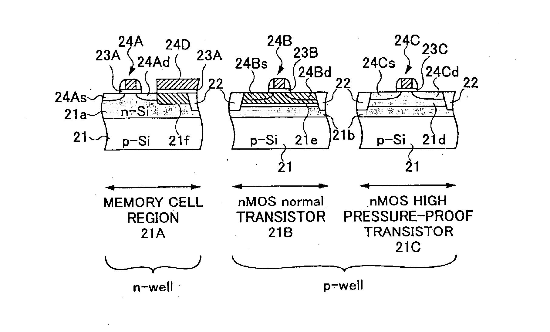
A description will now be given, with reference to FIGS. 2A through 2E, of a semiconductor integrated circuit apparatus according to the present invention.

FIGS. 2A through 2E show a fabrication process of the semiconductor integrated circuit apparatus according to the first embodiment.

Referring to FIGS. 2A through 2E, element regions 21A through 21C are defined on a p-type Si substrate 21 by an element separation structure 22 such as an STI structure. The element region 21A has an n-type well 21a.

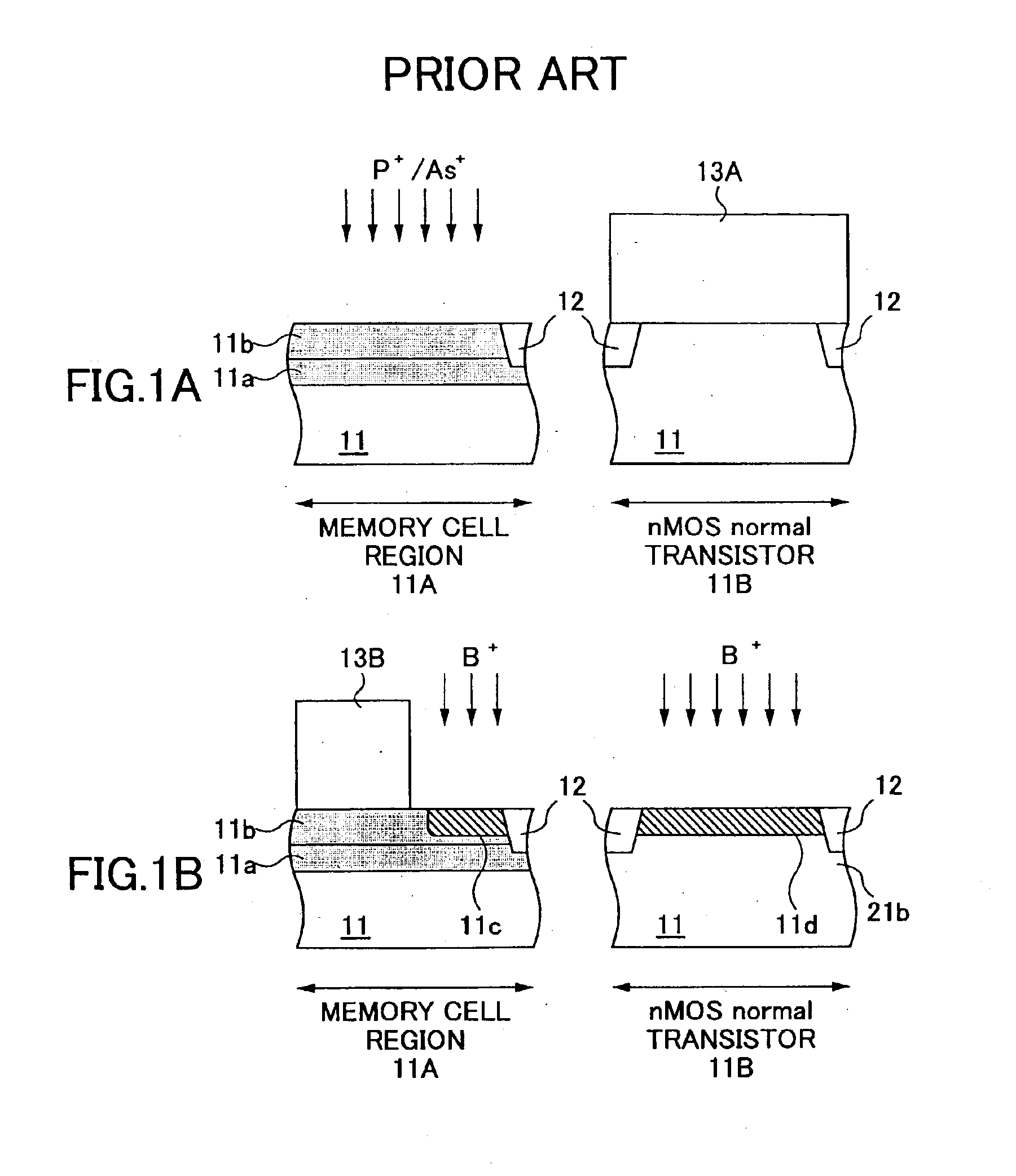
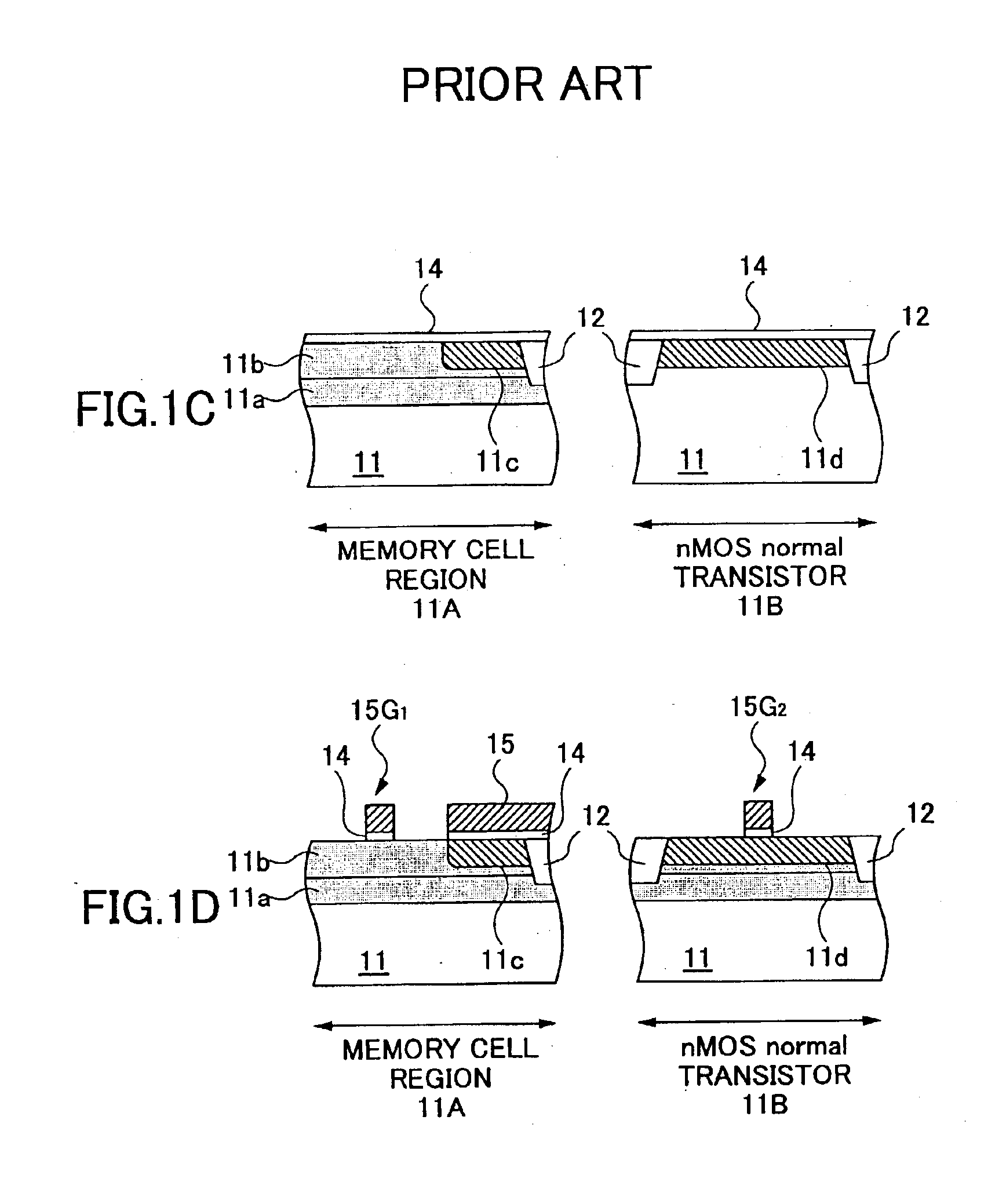
In a process in FIG. 2A, a resist pattern R1 covers the element region 21A having the n-type well 21a. When ions of a p-type impurity element such as B are implanted into the element regions 21A through 21C, for instance, at an acceleration voltage of 300 keV with a dose of 3×10¹² ions / cm2 by using the resist pattern R1 as a mask, it is possible to form p-type wells 21b in the element regions 21B and 21C. Subsequently, when the ions of the p-type impurity element are implanted at an accele...

second embodiment

A description will now be given, with reference to FIG. 4A through 4E, of a semiconductor integrated circuit apparatus fabrication process according to the present invention.

FIGS. 4A through 4E show a fabrication process of the semiconductor integrated circuit apparatus according to the second embodiment.

Referring to FIGS. 4A through 4E, element regions 31A through 31C are defined on a p-type Si substrate 31 by an element separation structure 32 such as an STI structure. In a process in FIG. 4A, P ions are uniformly implanted into the element regions 31A through 31C, for instance, at an acceleration voltage of 500 keV with a dose of 3×10¹² ions / cm2. As a result, an n-type well 31a is formed in each of the element regions 31A through 31C. Subsequently, As ions are uniformly implanted into the element regions 31A through 31C, for instance, at an acceleration voltage of 150 keV with a dose of 5×10¹² ions / cm2. As a result, it is possible to form n-type regions 31b having a predetermined...

third embodiment

A description will now be given, with reference to FIGS. 5A through 5G, of a fabrication process of a semiconductor integrated circuit apparatus according to the present invention.

FIGS. 5A through 5G show the fabrication process of the semiconductor integrated circuit apparatus according to the third embodiment.

Referring to FIGS. 5A through 5G, a memory cell region 41A, an element region 41B where an nMOS transistor, a part of a CMOS logic element, is to be formed, an element region 41C where a high pressure-proof nMOS transistor is to be formed, an element region 41D where a pMOS transistor, another part of the CMOS logic element, is to be formed, and an element region 41E where a high pressure-proof pMOS transistor is to be formed are defined on a p-type Si substrate 41 by an element separation structure 42 such as an STI structure.

In a process in FIG. 5A, a resist pattern R4 covers the element regions 41B and 41C. In order to form an n-type well 41a, P ions are implanted into the...


PUM


Abstract

A semiconductor integrated circuit apparatus having a planar capacitor can use a plurality of source voltages therein. According to the semiconductor integrated circuit apparatus, it is possible to not only control thresholds of individual MOS transistors but also reduce the threshold voltage of the planar capacitor without any additional fabrication process. The semiconductor integrated circuit apparatus includes a p-channel memory transistor and a capacitor in a first n-type element region, an n-channel low-voltage MOS transistor in a second p-type element region, and an n-channel high-voltage MOS transistor in a third p-type element region. A channel region of the second MOS transistor is doped under a high density profile by using a p-type impurity element. At the same time, the p-type impurity element is imported in a capacitor region of the first element region under the substantially same profile.

Description

CROSS-REFERENCE TO RELATED APPLICATIONSThe present application is based on Japanese priority application No. 2002-193821 filed Jul. 2, 2002, the entire contents of which are hereby incorporated by reference.BACKGROUND OF THE INVENTION1. Field of the InventionThe present invention generally relates to a semiconductor apparatus, and more particularly to a semiconductor apparatus that has a planar capacitor.2. Description of the Related ArtThere is a DRAM (Dynamic Random Access Memory) among fundamental semiconductor apparatuses. In general, the DRAM comprises a single transistor and a single capacitor. In particular, when a DRAM uses a planar capacitor as the capacitor, the structure of the planar DRAM is quite suitable to miniaturization. For this reason, such a planar DRAM is used as a semiconductor memory apparatus. Furthermore, it has been recently attempted to have the planar DRAM serve as a substitute for a high speed memory SRAM (Static Random Access Memory) in a high speed CMO...

Claims


Application Information

Patent Timeline
IPC IPC(8): H01L27/105H01L27/04H01L21/822H01L21/8234H01L21/8242H01L27/06H01L27/10H01L27/108
CPCH01L27/1085H01L27/10897H01L27/10894H01L27/10885Y10S257/906H10B12/03H10B12/09H10B12/50H10B12/482H01L27/10
Inventor ANEZAKI, TORU
Owner FUJITSU LTD
Why Eureka
Try Eureka