Passivation contact solar cell and preparation method thereof

A technology for solar cells and passivation layers, applied in the field of solar cells, can solve problems such as process limitations and inability to make a suede surface, and achieve the effects of reducing the recombination rate, improving the light utilization rate, and the method is simple

Inactive Publication Date: 2020-06-12
TAIZHOU ZHONGLAI PHOTOELECTRIC TECH CO LTD
View PDF4 Cites 3 Cited by
  • Summary
  • Abstract
  • Description
  • Claims
  • Application Information

AI Technical Summary

Problems solved by technology

[0004] The existing pyramid suede preparation process for n-type passivated contact cells is a double-sided process. Due to the limitation of the process, it is impossible to make a structure with one side suede and one side mirror.

Method used


Image

  • Passivation contact solar cell and preparation method thereof
  • Passivation contact solar cell and preparation method thereof
  • Passivation contact solar cell and preparation method thereof

Examples


preparation example Construction

[0045] A kind of preparation method of passivated contact solar cell provided by the invention comprises the following steps:

[0046] (1), preparing a tunneling oxide layer on the back surface of the N-type crystalline silicon substrate, and preparing a phosphorus-doped polysilicon layer on the tunneling oxide layer;

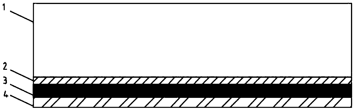
[0047] (2), preparing silicon nitride anti-reflection layer on the phosphorus-doped polysilicon layer on the back surface of the N-type crystalline silicon substrate; the silicon nitride anti-reflection layer is also used as a mask on the back surface of the N-type crystalline silicon substrate;

[0048] (3), put the N-type crystalline silicon substrate into the alkaline solution, and carry out alkali-texturing treatment on the front surface of the N-type crystalline silicon substrate. During the treatment, the silicon nitride mask on the back surface of the N-type crystalline silicon substrate is Thin;

[0049] (4), performing boron diffusion treatment on the...

Embodiment 1

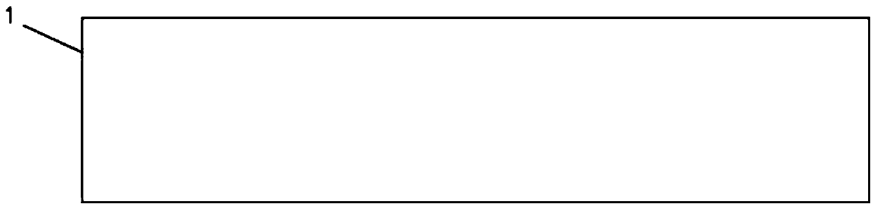
[0069] (1) Take an N-type crystalline silicon substrate 1 with a resistivity of 1Ω·cm and a thickness of 170 μm, and place the N-type crystalline silicon substrate 1 with a resistivity of 1Ω·cm and a thickness of 170 μm in a 20wt% NaOH solution , at a temperature of 85° C., reacting for 130 s to form double-sided mirror polishing, and the reflectance of the treated N-type crystalline silicon substrate 1 is 36%. Complete the battery structure of this step as figure 1 shown.

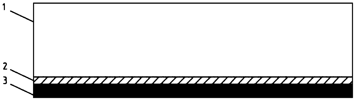
[0070] (2) On the back surface of the N-type crystalline silicon substrate 1, a thermal oxidation method is used to prepare a tunneling oxide layer 2 with silicon dioxide as a material. The thickness of the tunneling oxide layer 2 is nm. On the tunneling oxide layer 2, first The polysilicon layer is prepared by low-pressure chemical deposition, the deposition temperature is 600° C., and the thickness of the polysilicon layer is 100 nm; then, the polysilicon is doped and annealed by ion implantation to for...

Embodiment 2

[0078] (1) Take an N-type crystalline silicon substrate 1 with a resistivity of 1Ω·cm and a thickness of 170 μm, and place the N-type crystalline silicon substrate 1 with a resistivity of 1Ω·cm and a thickness of 170 μm in a KOH solution with a mass concentration of 20 wt % , at a temperature of 90° C., reacting for 200 s to form double-sided mirror polishing, and the reflectance of the treated N-type crystalline silicon substrate 1 is 39%. Complete the battery structure of this step as figure 1 shown.

[0079] (2) HNO is used on the back surface of the N-type crystalline silicon substrate 1 3 The oxidation method uses silicon dioxide as the material to prepare the tunneling oxide layer 2. The thickness of the tunneling oxide layer 2 is 2nm. On the tunneling oxide layer 2, a polysilicon layer is first prepared by low-pressure chemical deposition. The thickness of the layer is 200nm; then the polysilicon is doped by ion implantation and annealed to form the phosphorus-doped p...


PUM

PropertyMeasurementUnit
thicknessaaaaaaaaaa
thicknessaaaaaaaaaa
thicknessaaaaaaaaaa

Abstract

The invention relates to a passivation contact solar cell and a preparation method thereof. The solar cell comprises an N-type crystalline silicon substrate, wherein the front surface of the N-type crystalline silicon substrate sequentially comprises an emitter layer, an aluminum oxide passivation layer, a silicon nitride antireflection layer and a metal slurry layer from bottom to top; wherein the back surface of the N-type crystalline silicon substrate sequentially comprises a tunneling oxide layer, a phosphorus-doped polycrystalline silicon layer, a silicon nitride antireflection layer anda metal slurry layer from bottom to top. According to the solar cell, the open-circuit voltage and the short-circuit current of the cell can be remarkably improved, so that the efficiency of an n-typepassivation contact cell can be improved; moreover, the light utilization rate can also be improved, the back surface recombination rate is reduced, the cell efficiency is improved by 0.15% or above,meanwhile, additional process steps do not need to be added, and the method is simple and suitable for mass production.

Description

technical field [0001] The invention relates to the technical field of solar cells, in particular to a passivated contact solar cell and a preparation method thereof. Background technique [0002] The n-type battery uses n-type silicon as the substrate material, which has good resistance to metal impurity pollution and long minority carrier diffusion length. Compared with the traditional p-type battery, it has the advantages of no light-induced attenuation and higher battery efficiency. favored by the market. The n-type passivated contact battery is a new type of n-type battery structure. The tunneling passivation layer provides good surface passivation for the n+ surface, greatly reduces the metal contact recombination, and improves the open circuit voltage and short circuit current of the battery. The cell efficiency of this structure is much higher than that of traditional crystalline silicon cell products, which is more conducive to reducing the cost of photovoltaic pow...

Claims


Application Information

Patent Timeline
Patent Type & Authority Applications(China)
IPC IPC(8): H01L31/18H01L31/0216H01L31/0236
CPCH01L31/02167H01L31/02168H01L31/02366H01L31/1876Y02E10/50Y02P70/50
Inventor 陆俊宇季根华陈嘉林建伟
Owner TAIZHOU ZHONGLAI PHOTOELECTRIC TECH CO LTD
Why Eureka
Try Eureka