Nitride semiconductor epitaxial structure

A technology of nitride semiconductor and epitaxial structure, which is applied in the direction of semiconductor devices, electrical components, circuits, etc., can solve problems such as the mismatch between crystal lattice and thermal expansion coefficient, and achieve the goal of increasing product yield, relieving stress, and improving the quality of gallium nitride Effect

Pending Publication Date: 2022-07-29
南京百识电子科技有限公司
View PDF8 Cites 0 Cited by
  • Summary
  • Abstract
  • Description
  • Claims
  • Application Information

AI Technical Summary

Problems solved by technology

[0005] Purpose of the invention: The purpose of the invention is to provide a nitride semiconductor epitaxial structure to solve the problem of mismatch between the lattice and thermal expansion coefficient between gallium nitride and silicon substrate, so as to reduce chip cracking and avoid the generation of defects

Method used


Image

  • Nitride semiconductor epitaxial structure
  • Nitride semiconductor epitaxial structure
  • Nitride semiconductor epitaxial structure

Examples


Embodiment Construction

[0024] The present invention will be further described below with reference to the accompanying drawings and embodiments.

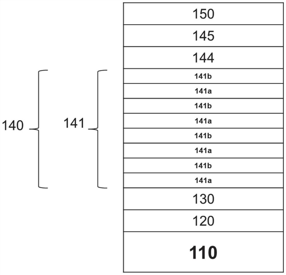
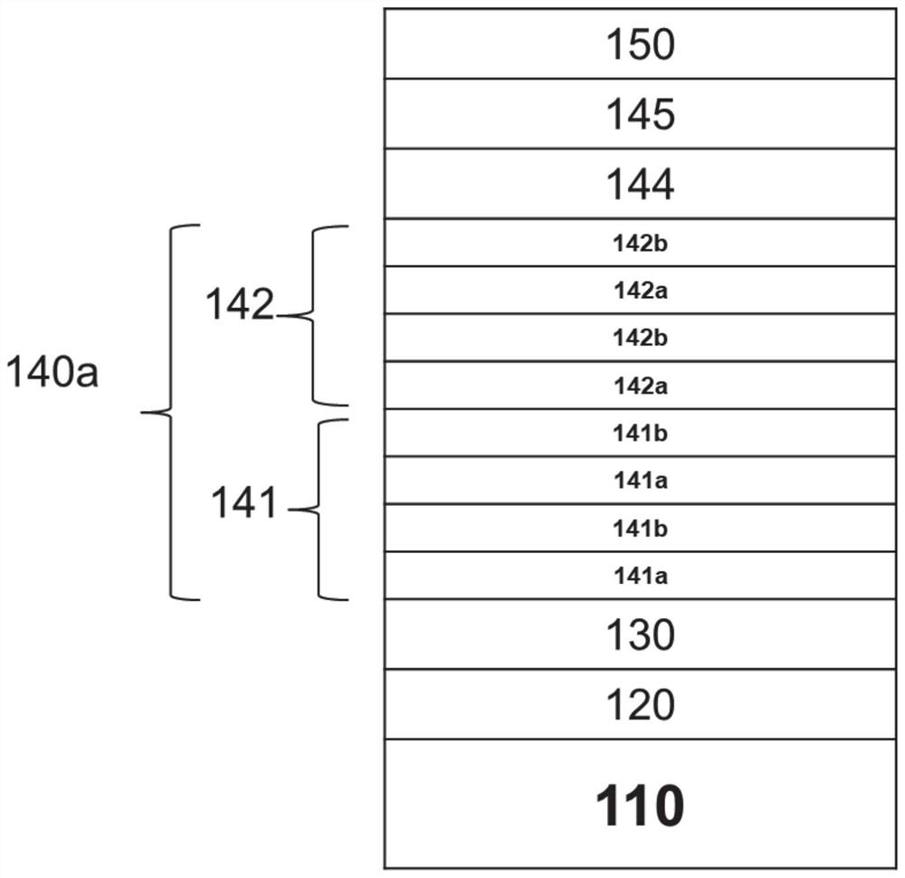
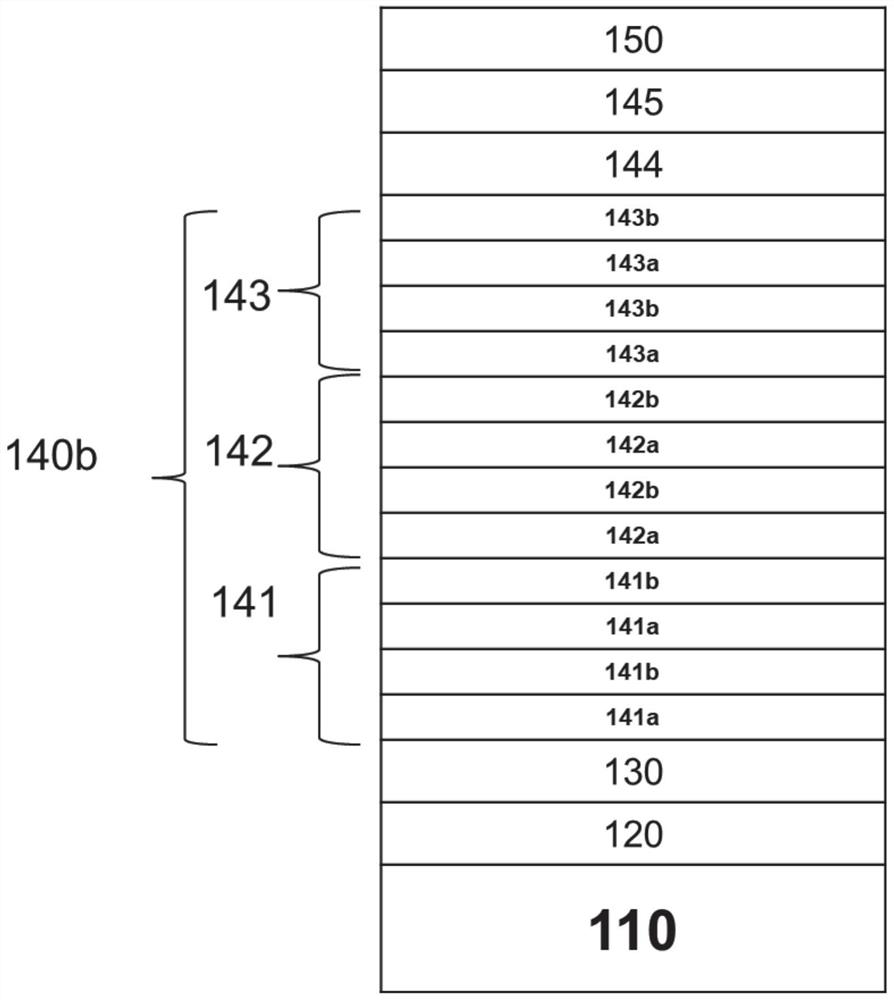
[0025] figure 1 It is a schematic cross-sectional view of a nitride semiconductor epitaxial structure according to an embodiment of the present invention, wherein the first superlattice composite buffer layer schematically shows several overlapping layers of the first Aly1GaN layer and several layers of the first GaN layer. layer, not representing its actual number of layers.

[0026] see figure 1 In this embodiment, the nitride semiconductor structure 100 includes a substrate 110, a nucleation layer 120, a transition layer 130, and a composite buffer structure 140, wherein the material of the substrate 110 may include silicon, aluminum oxide or glass. Taking a silicon substrate as an example, the substrate 110 may be a patterned silicon substrate, and the pattern may be a regular or irregular micro-pattern or nano-pattern. For example, after the subst...


PUM

PropertyMeasurementUnit
thicknessaaaaaaaaaa
thicknessaaaaaaaaaa
thicknessaaaaaaaaaa

Abstract

The invention discloses a nitride semiconductor epitaxial structure, which comprises a substrate, a nucleating layer, a transition layer, a composite buffer layer, a top gallium nitride layer and a coating layer are sequentially arranged on the substrate, the transition layer is an AlxGaN layer, the composite buffer layer comprises a first composite buffer layer, the first composite buffer layer comprises a plurality of Aly1GaN layers and a plurality of GaN layers which are mutually overlapped, y1 is greater than x, and y2 is greater than x. The Aly1GaN layers in the first composite buffer layer are the same in thickness, and the first GaN layers are the same in thickness. According to the method, the epitaxial layer is grown through superlattices, warping can be effectively controlled, the quality of gallium nitride is improved, defects are reduced, the product yield is increased, in the growth method of the superlattice composite buffer structure, different aluminum content growth modes are added, warping can be further effectively improved, and the product yield is increased.

Description

technical field [0001] The invention relates to a semiconductor structure, in particular to a nitride semiconductor epitaxial structure. Background technique [0002] In the nitride semiconductor structure, since silicon has the advantages of higher thermal conductivity and lower cost than sapphire substrates, large-scale nitride semiconductors based on silicon substrates have become the most important choice in nitride power devices. important components. However, taking a gallium nitride (GaN) semiconductor layer as an example, the lattice difference between the gallium nitride semiconductor layer and the silicon substrate is 17%, and the difference in thermal expansion coefficient therebetween is 54%. The above difference not only causes film cracking due to excessive thermal stress during cooling, but also causes internal stress in the gallium nitride semiconductor layer during the epitaxial growth process, thereby causing film cracking and forming defects. Therefore, ...

Claims


Application Information

Patent Timeline
Patent Type & Authority Applications(China)
IPC IPC(8): H01L29/06H01L29/15H01L29/20H01L29/201
CPCH01L29/0684H01L29/15H01L29/2003H01L29/201
Inventor 胡智威蔡清富蔡长祐陈威佑
Owner 南京百识电子科技有限公司
Why Eureka
Try Eureka