Graphite film surface etching method
A surface etching and graphite film technology, applied in the direction of graphite, can solve the problems of cumbersome post-processing, difficult to apply on a large scale, and achieve the effect of improving surface roughness, improving bonding force and broad application prospects.
- Summary
- Abstract
- Description
- Claims
- Application Information
AI Technical Summary
Problems solved by technology
Method used
Image
Examples
Embodiment 1
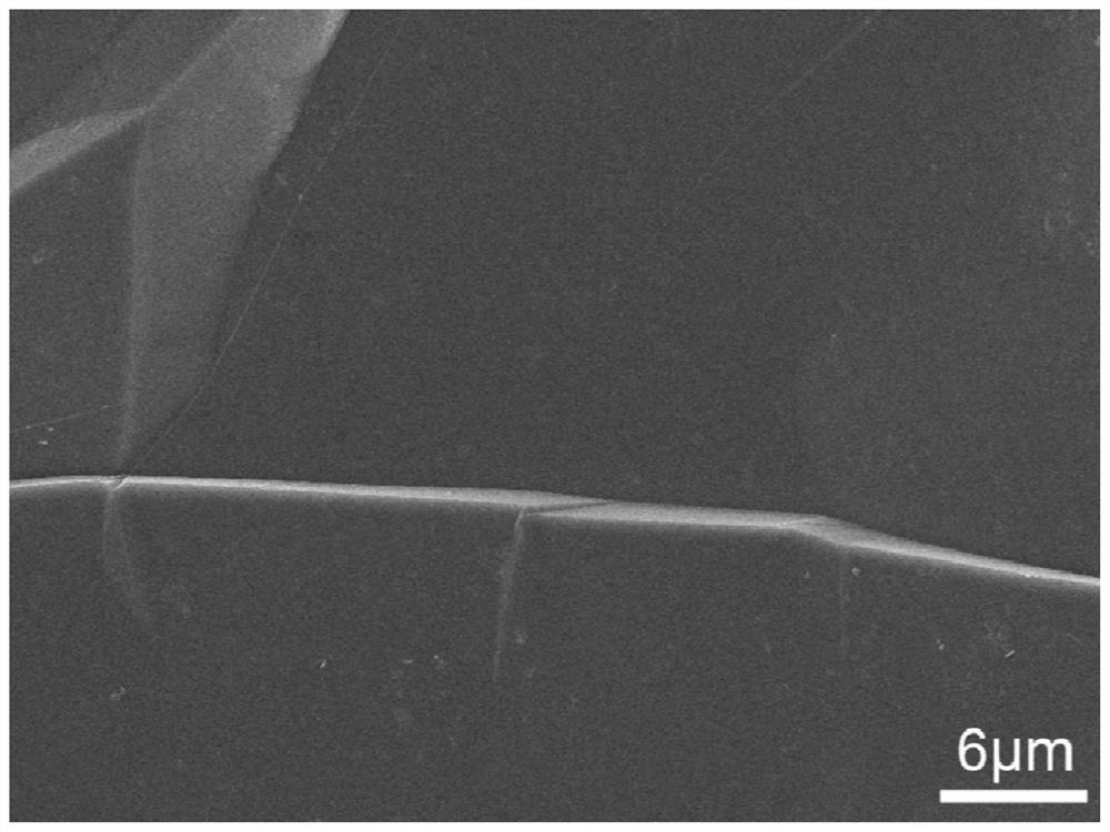
[0024] (1) Cut an artificial high thermal conductivity graphite film with a thickness of 70 μm into a size of 150*100 mm and place it in anhydrous ethanol to ultrasonically remove the adsorbed impurities on the surface of the graphite film, then use deionized water to wash off the ethanol on the surface of the graphite film Dry in a vacuum oven at 80°C.
[0025] (2) The graphite film is placed in a tube furnace, and the nitrogen-oxygen mixed gas (oxygen volume fraction is 21%) flows through the tube furnace, and the temperature is 650°C.
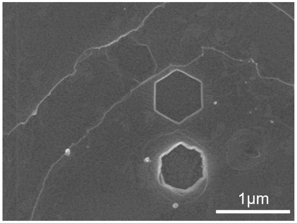
[0026] (3) The graphite film was kept in an atmosphere of 650° C. for 90 minutes, and then the heating was stopped, and the graphite film was taken out immediately, and then the graphite film was stored in a dry environment at room temperature. In this example, the surface of the graphite film obtained generally has six-membered annular pits and long grooves with a diameter of 500-800 nm, and a depth of 50-80 nm.
Embodiment 2
[0028] The etching time in the high temperature atmosphere was reduced to 30 min, and other conditions were the same as in Example 1. The surface of the obtained graphite film generally had six-membered annular pits and long grooves with a diameter of 200-400 nm and a depth of 10-30 nm.
Embodiment 3
[0030] The high-temperature atmosphere etching time was extended to 150min, and other conditions were the same as those in Example 1. The surface of the obtained graphite film generally had six-membered annular pits and long grooves with a diameter of 1000-1500nm and a depth of 100-120nm.
PUM
| Property | Measurement | Unit |
|---|---|---|
| thickness | aaaaa | aaaaa |
| diameter | aaaaa | aaaaa |
| diameter | aaaaa | aaaaa |
Abstract
Description
Claims
Application Information

