Silicon carbide wafer back surface processing technology

A processing technology, silicon carbide technology, used in sustainable manufacturing/processing, final product manufacturing, semiconductor/solid-state device manufacturing, etc., which can solve the problems of high wafer fragmentation rate and large grinding volume.

Active Publication Date: 2022-08-09
成都功成半导体有限公司
View PDF12 Cites 2 Cited by
  • Summary
  • Abstract
  • Description
  • Claims
  • Application Information

AI Technical Summary

Problems solved by technology

[0004] The invention provides a silicon carbide wafer backside process processing technology, which solves the problems of large grinding amount and high

Method used


Image

  • Silicon carbide wafer back surface processing technology
  • Silicon carbide wafer back surface processing technology
  • Silicon carbide wafer back surface processing technology

Examples


Embodiment

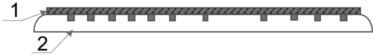
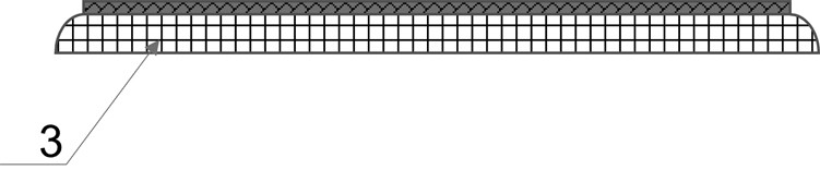
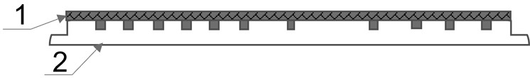
[0059] like Figure 1-Figure 7 As shown, a backside manufacturing process of a silicon carbide wafer specifically includes the following steps:

[0060] S1. The first SiC carrier 3 and the SiC wafer 2 that has completed the front-side process are thermally oxidized to SiO 2 Layer 1 growth; thermal oxidation of SiO 2 Layer 1 is grown to a thickness of 100-150 nm; as Figure 1-2 shown;

[0061] S2. Trimming process for SiC wafer 2: In order to ensure the quality of subsequent wafer thinning, the wafer trimming depth should be greater than the same wafer thinning thickness, and the wafer trimming depth range is between 100-200um; The stability of the wafer trimming process. In step S2, the wafer trimming can be performed by multiple trimming methods. The width of each trimming does not exceed 2mm and the depth does not exceed 100um. The specific steps are:

[0062] Step S201, trimming the SiC wafer 2 for the first time, the trimming width is 2mm, and the depth is 100um;

[0...


PUM

PropertyMeasurementUnit
Thicknessaaaaaaaaaa

Abstract

The invention discloses a silicon carbide wafer back surface processing technology, which comprises the following steps: carrying out a multi-step edge trimming technology on a silicon carbide wafer substrate before silicon carbide bonding, and then carrying out a wafer bonding technology, a wafer multi-time thinning polishing and annealing technology, a wafer back surface technology, a wafer de-bonding technology and a wafer high-temperature annealing technology. And finally, carrying out a wafer bonding process and a wafer secondary trimming process. By the adoption of the technological process, the risks of breaking and burning of the SiC wafer in the thinning process are greatly reduced, and the back face process and the high-temperature tempering process of the silicon carbide wafer substrate can be safely and effectively completed.

Description

technical field [0001] The invention relates to the technical field of semiconductor processing, in particular to a backside manufacturing process of a silicon carbide wafer. Background technique [0002] With the rapid development of semiconductor technology, silicon carbide (Silicon Carbide, SiC) material has become a new generation of popular semiconductor materials due to its wide band gap, high electron mobility and high thermal conductivity. Due to the update and iteration of electronic devices, the market has put forward higher requirements for the on-voltage drop of semiconductor devices. Therefore, it is required to thin the silicon carbide wafer after the front-side process is completed to reduce the drift layer thickness of the device. Thereby reducing the turn-on voltage drop of the device. In addition, with the further complexity of the device structure design, it also puts forward more demands on the backside processing technology of the silicon carbide proces...

Claims


Application Information

Patent Timeline
IPC IPC(8): H01L21/304H01L21/04H01L21/324H01L21/67H01L29/16
CPCH01L21/304H01L21/045H01L21/324H01L21/67092H01L29/1608Y02P70/50
Inventor 唐义洲
Owner 成都功成半导体有限公司
Why Eureka
Try Eureka