Novel packaging system chip NPSC architecture based on wireless high-speed bus
A high-speed bus, packaging system technology, applied in the architecture with a single central processing unit, semiconductor/solid-state device components, semiconductor devices, etc., to achieve the effect of high yield, low cost, and wide bandwidth
- Summary
- Abstract
- Description
- Claims
- Application Information
AI Technical Summary
Problems solved by technology
Method used
Image

Examples
Embodiment 1
[0049] refer to image 3 As shown, this embodiment provides a novel NPSC architecture of a packaging system chip based on a wireless high-speed bus, which is formed by stacking one or more chiplets on each other or stacking the one or more chiplets and one or more memory dies on each other; Wherein, the one or more chiplets are integrated with a silicon-based optical transceiver IP module, and the silicon-based optical transceiver IP module integrated by the one or more chiplets is connected to the same laser generator.
[0050] One or more chiplets of this embodiment are stacked on top of each other or the one or more chiplets and one or more memory dies are stacked on top of each other or side-by-side on top of an interposer with TSVs.
[0051] In the preferred implementation of this embodiment, an interposer with through-silicon vias is provided on the substrate, and further package bumps are provided on the interposer with through-silicon vias.
[0052] The interposer wit...
Embodiment 2
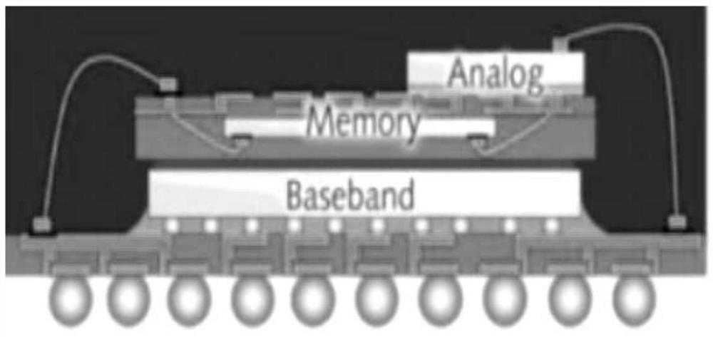
[0058] On the basis of Embodiment 1, this embodiment uses 2.5D packaging technology to package the new packaging system chip NPSC architecture based on wireless high-speed bus. For details, see Figure 4 , where the stiffener is the stiffener; the Substrate is the substrate; the interposer is the silicon interposer; the bump is the bump; u-bump is the micro-bump.
[0059] In the novel packaged system-on-chip of the present embodiment, chiplets are stacked together or stacked with memory dies, and there is no need to build a complex system-on-chip.
[0060] The 2.5D packaging in this embodiment is an upgrade of the traditional 2DIC packaging technology, which can realize more precise circuit and space utilization.
[0061] In the 2.5D package of this embodiment, the dies are stacked or placed side by side on top of an interposer with through-silicon vias (TSV: ThroughSiliconVia).
[0062] This embodiment has a signal redistribution interconnection layer (RDL) between the dies ...
Embodiment 3
[0065] On the basis of Embodiment 2, this embodiment further uses 3D packaging technology to package the NPSC architecture of the new packaging system chip based on the wireless high-speed bus. For details, see Figure 5 , it can be seen from the cross-sectional view of the 3D package that the vertical interconnection between silicon chips is achieved through metal copper TSVs.
[0066] The 3D package in this embodiment mainly uses metal-metal bonding to realize multi-layer vertical interconnection. The Cu-Sn bonding principle in this embodiment is: after the temperature rises, the metal Sn melts and reacts with Cu to form a metastable metal-to-metal bond. Compound CuSns (melting point 415 ℃), and then Cu, Sns and Cu further react to form the stable intermetallic compound CuzSn251 (melting point 676 ℃).
[0067] In this embodiment, since the melting point of the alloy phase is higher than the Cu-Sn eutectic bonding temperature, when the multilayer chips are stacked, the heatin...
PUM
| Property | Measurement | Unit |
|---|---|---|
| Roughness | aaaaa | aaaaa |
Abstract
Description
Claims
Application Information
 - R&D
- Intellectual Property
- Life Sciences
- Materials
- Tech Scout
- Unparalleled Data Quality
- Higher Quality Content
- 60% Fewer Hallucinations
Browse by: Latest US Patents, China's latest patents, Technical Efficacy Thesaurus, Application Domain, Technology Topic, Popular Technical Reports.
© 2025 PatSnap. All rights reserved.Legal|Privacy policy|Modern Slavery Act Transparency Statement|Sitemap|About US| Contact US: help@patsnap.com