
Semiconductor device with conduction voltage drop self-clamping and preparation method thereof

A conduction voltage drop, semiconductor technology, applied in semiconductor/solid-state device manufacturing, semiconductor devices, electrical components, etc., can solve the problems of insufficient reliability of MPS structure, small safe working area, low softness, etc., and achieve stable clamping conduction Low voltage drop, low static leakage, and the effect of curbing surge current

Active Publication Date: 2022-08-09
VANGUARD SEMICON CORP
View PDF8 Cites 4 Cited by
  • Summary
  • Abstract
  • Description
  • Claims
  • Application Information

AI Technical Summary

Problems solved by technology

[0003] The technical problem to be solved by the present invention is to overcome the defects of low softness and high loss in the traditional planar structure of fast recovery diodes in the prior art, while the safe working area of ​​the traditional CIC structure is small, and the reliability of the traditional MPS structure is insufficient, thereby providing a A semiconductor device with conduction voltage drop self-clamping and its preparation method

Method used


Image

  • Semiconductor device with conduction voltage drop self-clamping and preparation method thereof
  • Semiconductor device with conduction voltage drop self-clamping and preparation method thereof

Examples


Embodiment Construction

[0036] In order to make those skilled in the art better understand the technical solutions in the present application, the technical solutions in the embodiments of the present application will be described clearly and completely below with reference to the accompanying drawings in the embodiments of the present application. Obviously, the described implementation The examples are only some of the embodiments of the present application, but not all of the embodiments. Based on the embodiments in this application, all other embodiments obtained by those of ordinary skill in the art without creative efforts shall fall within the protection scope of this application.

[0037] In the description of the present invention, it should be noted that the terms "center", "upper", "lower", "left", "right", "vertical", "horizontal", "inner", "outer", etc. The indicated orientation or positional relationship is based on the orientation or positional relationship shown in the accompanying dr...


PUM


Abstract

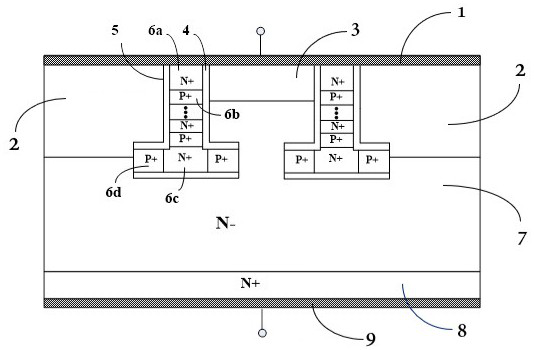
The invention belongs to the technical field of power semiconductor devices, and particularly relates to a semiconductor device with conduction voltage drop self-clamping and a preparation method thereof. Compared with a traditional fast recovery diode structure, the Zener diode structure capable of achieving self-clamping voltage drop is integrated, the first N-type polycrystalline silicon and the first P-type polycrystalline silicon are longitudinally and alternately arranged on the upper portion in the groove, the second N-type polycrystalline silicon and the second P-type polycrystalline silicon are transversely and alternately arranged on the lower portion in the groove, the device is integrated with the Zener diode in reverse parallel connection, and therefore the device can achieve self-clamping voltage drop. When large surge current is generated, the Zener breakdown characteristic can be used for clamping conduction voltage drop, so that the device is prevented from being damaged; by arranging the inverted T-shaped groove between the body region and the P-type heavily doped region, the P-type heavily doped region with relatively shallow junction depth can be shielded in a dynamic reverse recovery process, so that the P-type heavily doped region is effectively protected, and a reverse bias safe working area (RBSOA) of the device is increased.

Description

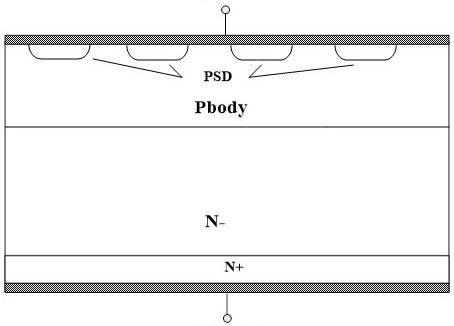
technical field [0001] The invention belongs to the technical field of power semiconductor devices, and particularly relates to a semiconductor device with self-clamping on voltage drop and a preparation method thereof. Background technique [0002] Fast recovery diodes traditional traditional planar structures such as figure 2 As shown, the process fabrication successively forms a P-type lightly doped body region (Pbody) and a P-type heavily doped region (PSD), and combines Pt doping or electron irradiation to control the minority carrier lifetime, thereby achieving the expected turn-on voltage drop and reverse recovery loss; the traditional CIC structure reduces the area of ​​the body region and forms part of the PSD region between the separated body regions to achieve dynamic optimization to improve softness and reduce loss, but this structure will cause The RBSOA (reverse bias safe operating area) of the device is reduced, resulting in a narrowing of the safe operating ...

Claims


Application Information

Patent Timeline
Patent Type & Authority Applications(China)
IPC IPC(8): H01L29/866H01L21/329H01L29/06H01L29/45
CPCH01L29/866H01L29/0619H01L29/456H01L29/66106
Inventor 李伟聪伍济
Owner VANGUARD SEMICON CORP
Learn More