

Semiconductor device and its mfg. method
A semiconductor and device technology, applied in the field of semiconductor devices, can solve problems such as long time, distortion, large substrate, etc.
- Summary
- Abstract
- Description
- Claims
- Application Information
AI Technical Summary
Problems solved by technology
Method used
Image

Examples
Embodiment 1
[0064] In this embodiment, a complementary circuit is composed of a P-channel TFT (PTFT) and an N-channel TFT (NTFT) both made of crystalline silicon film on a glass substrate. The structure of this embodiment can be applied to the switching device of the pixel electrode of the active matrix liquid crystal display, its peripheral driving circuit, image sensor and integrated circuit. Also, devices to which this embodiment is applied are not limited to insulated gate field effect transistors. They can be other transistors and diodes. The present invention is applicable to integrated circuits including semiconductor devices, resistors, and capacitors.
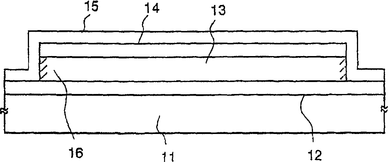
[0065] Figure 1(A)~1(D) and 2(A) to 2(B) are cross-sectional views of TFTs manufactured according to this embodiment, and are used to illustrate process steps. First, silicon oxide was sputtered as a 2000 Å thick base film 12 on a substrate 11 made of Corning 7059. Then, a well-known amorphous silicon film 13 is formed to a t...
Embodiment 2
[0080] This embodiment relates to an active matrix liquid crystal display having N-channel TFTs used as switching devices for pixels. In the following description, only one pixel is discussed. Many other pixels (often hundreds or thousands) form the same. Obviously, N-channel TFTs can also be replaced by P-channel TFTs. The TFTs can also be used in peripheral circuits other than just the pixel unit of a liquid crystal display, and the TFTs can be used in pixel sensors or other devices.
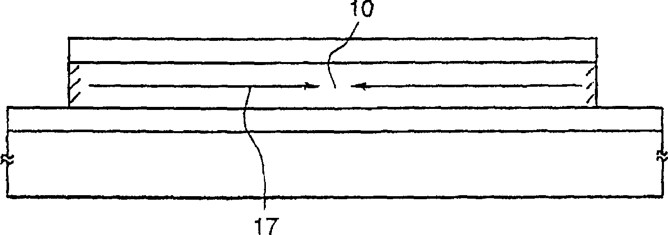
[0081] The process steps of the present embodiment are shown in Figure 1(A)~1(D) And 3(A)~3(B). The fabrication steps are performed in this order. In this embodiment, Corning 7059 with a thickness of 1.1 mm and a size of 300 mm×400 mm is used as the substrate 201 . Figure 1(A)~1(D) The steps shown are the same as those of Example 1, and therefore, these steps will not be described below.
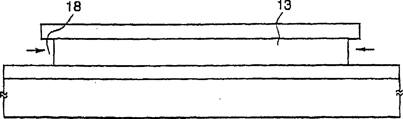
[0082] As shown in FIG. 1(D), after the crystallized silicon film 13 is obtained, individual devi...
Embodiment 3
[0088] In this embodiment, using a crystalline silicon film formed on a glass substrate, a P-channel TFT (PTFT) and an N-channel TFT (NTFT) are complementary combined to form a circuit. The structure of this embodiment can be applied to switching devices for pixel electrodes of active-matrix liquid crystal displays, peripheral drive circuits, image sensors, and integrated circuits.
[0089] The process steps of this embodiment are schematically shown in FIGS. 5(A) to 5(D). First, silicon oxide was sputtered onto a substrate 401 made of Corning 7059 as a base film 402 with a thickness of 200 Å. Next, a mask 403 made of metal, silicon oxide, and the like is formed. The mask 403 allows the base film 402 to expose the slit region. That is, when viewing the state shown in FIG. 5(A) from above, the slit-shaped parts of the base film 402 are exposed; while other parts are still covered. After forming the mask 403, a nickel silicide film is selectively formed on the region 400 with...
PUM
| Property | Measurement | Unit |
|---|---|---|
| Energy density | aaaaa | aaaaa |
| Energy density | aaaaa | aaaaa |
Abstract
Description
Claims
Application Information