Picture composition method, device, template and method for making same
A stencil and patterning technology, used in printing devices, printed circuit manufacturing, semiconductor/solid-state device manufacturing, etc., can solve problems such as the inability to form larger patterns
- Summary
- Abstract
- Description
- Claims
- Application Information
AI Technical Summary
Problems solved by technology
Method used
Image

Examples
no. 1 example
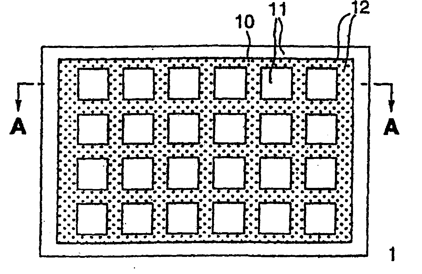
[0052] First, a method of forming a black matrix (masked pattern) used in a member such as a color filter or the like for a liquid crystal panel using a concave template as a first embodiment of the present invention will be described.
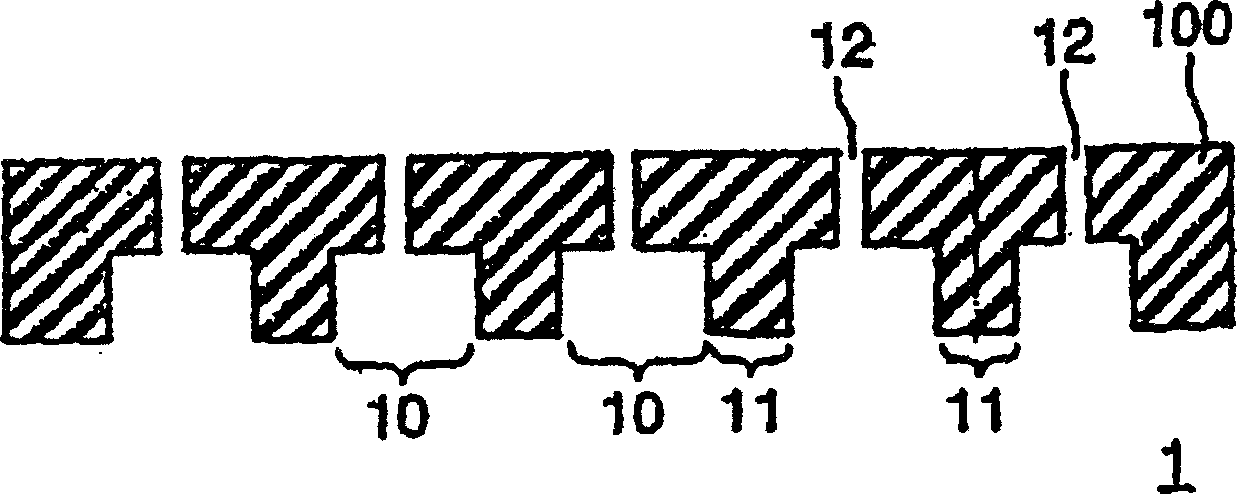
[0053] figure 1 Shown is a plan view of the graphic transfer surface of the stencil used in the present invention. figure 2 shown along figure 1 The cross-sectional view of the straight line A-A (section) in is used to illustrate the structure of this template.
[0054] like figure 1 and 2 As shown, the template 1 of the present embodiment has a pattern transfer surface ( figure 2 The structure of the concave part in the bottom). Formed in the pattern transfer area 10 through the rear surface of the original template 100 ( figure 2 A plurality of through holes 12 at the top). The inner wall of the through hole 12 is preferably polished or treated so as to exhibit non-affinity to liquid. If it is treated to have non-affinity, when no...
no. 2 example
[0087] Next, a method for forming a black matrix (masked pattern) used in a color filter of a liquid crystal panel or the like using a convex template as a second embodiment of the present invention will be described.
[0088] Figure 8 Shown is a plan view of the pattern transfer surface of the stencil used in this example. Figure 9 shown along Figure 8 A cross-sectional view of A-A (section) in , used to illustrate the template structure.
[0089] like Figure 8 and 9 As shown, the template 1b of this embodiment has an upwardly convex pattern transfer area 10b on the pattern transfer surface of the substrate template 100. in other words, Figure 8 The planar structure of the graphic transfer surface shown in figure 1 The structure shown is the same, but the graphic transfer area 10b corresponds to the raised portion of the template.
[0090] A plurality of through holes 12b passing through the rear surface of the substrate template 100 are formed in the pattern tran...
no. 3 example
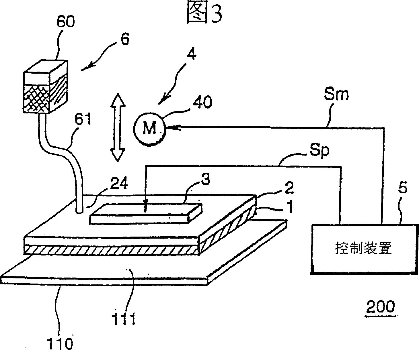
[0096] Next, a patterning apparatus capable of forming a desired pattern using an ink jet recording head will be described as a third embodiment of the present invention.
[0097] Figure 11 Shown is the configuration of the patterning device of this embodiment. like Figure 11 As shown, the patterning device 200b of this embodiment includes a template 1, an inkjet recording head 2b, a template delivery mechanism 4b, a control device 5b, a liquid storage mechanism 6b and an ejection head delivery mechanism 7.
[0098] Template 1 used in the first embodiment (see figure 1 and 2 ) can be used as it is as the template 1 in this embodiment, which can also use the template 1b used in the second embodiment. Since this embodiment particularly has a configuration in which a desired pattern can be formed by moving the ink jet recording head, the template can have a grid pattern or a uniform pattern composed of evenly spaced dots. According to a certain specification, the graphic t...
PUM
 Abstract
Description
Claims
Application Information
 - R&D
- Intellectual Property
- Life Sciences
- Materials
- Tech Scout
- Unparalleled Data Quality
- Higher Quality Content
- 60% Fewer Hallucinations
Browse by: Latest US Patents, China's latest patents, Technical Efficacy Thesaurus, Application Domain, Technology Topic, Popular Technical Reports.
© 2025 PatSnap. All rights reserved.Legal|Privacy policy|Modern Slavery Act Transparency Statement|Sitemap|About US| Contact US: help@patsnap.com