Frequency multiplier and semiconductor integrated circuit

A frequency multiplication circuit and circuit technology, applied in the direction of electrical components, modulation, transmission systems, etc., to achieve the effect of characteristic stabilization

Inactive Publication Date: 2004-09-22
KK TOSHIBA
View PDF0 Cites 0 Cited by
  • Summary
  • Abstract
  • Description
  • Claims
  • Application Information

AI Technical Summary

Problems solved by technology

For this reason, there is a limit to the miniaturization of circuits, and there is also a problem that countermeasures against interference waves must be taken

Method used


Image

  • Frequency multiplier and semiconductor integrated circuit
  • Frequency multiplier and semiconductor integrated circuit
  • Frequency multiplier and semiconductor integrated circuit

Examples


Embodiment 1

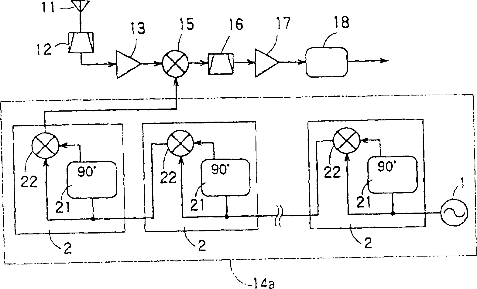
[0058] figure 1 It is a block diagram of Embodiment 1 of the receiver using the frequency multiplication circuit of the present invention. figure 1 The receiver, except for the source oscillation circuit 1 and the antenna 11, has been integrated into a single chip. in figure 1 In, for and Figure 15 The common parts are given the same reference numerals, and the differences are explained below.

[0059] figure 1 The frequency multiplier circuit, except the structure of the local oscillator circuit 14a that generates the local oscillator signal and Figure 15 The frequency multiplier circuit is different from Figure 15 The same composition.

[0060] figure 1 The local oscillation circuit 14a has a source oscillation circuit 1 that generates a source oscillation signal and a plurality of frequency multiplication circuits 2 connected in cascade. The frequency multiplier circuit 2 is actually a double frequency circuit that doubles the frequency of the input signal. A 90-degr...

Embodiment 2

[0110] In the first embodiment, when the shift of the phase shift by the phase shift circuit is not 90 degrees, the input waveform of the mixer contains a DC component. If a square wave is considered as a distorted wave, and when a square wave containing a DC component is multiplied by a mixer as an input waveform, in addition to (Equation 2), a square wave of the input signal will appear at the output of the frequency multiplier circuit. The frequency component of the wave. Consider the square wave as an even function when the interval from -X to +X is 1, and the other interval is -1, it can be expressed as

[0111] A(x-π / 2)+Asinxcosωt+A / 2·sin2xcos2ωt+A / 3·sin3xcos3ωt

[0112] +…+A / n·sinnxcosnωt

[0113] (Equation 3)

[0114] Among them, A is a constant, ω is the angular frequency 2πfL0, t is time, n is a natural number, and the first term is the DC component. For example, if n=2 and the source oscillation frequency is f0, the frequency output from th...
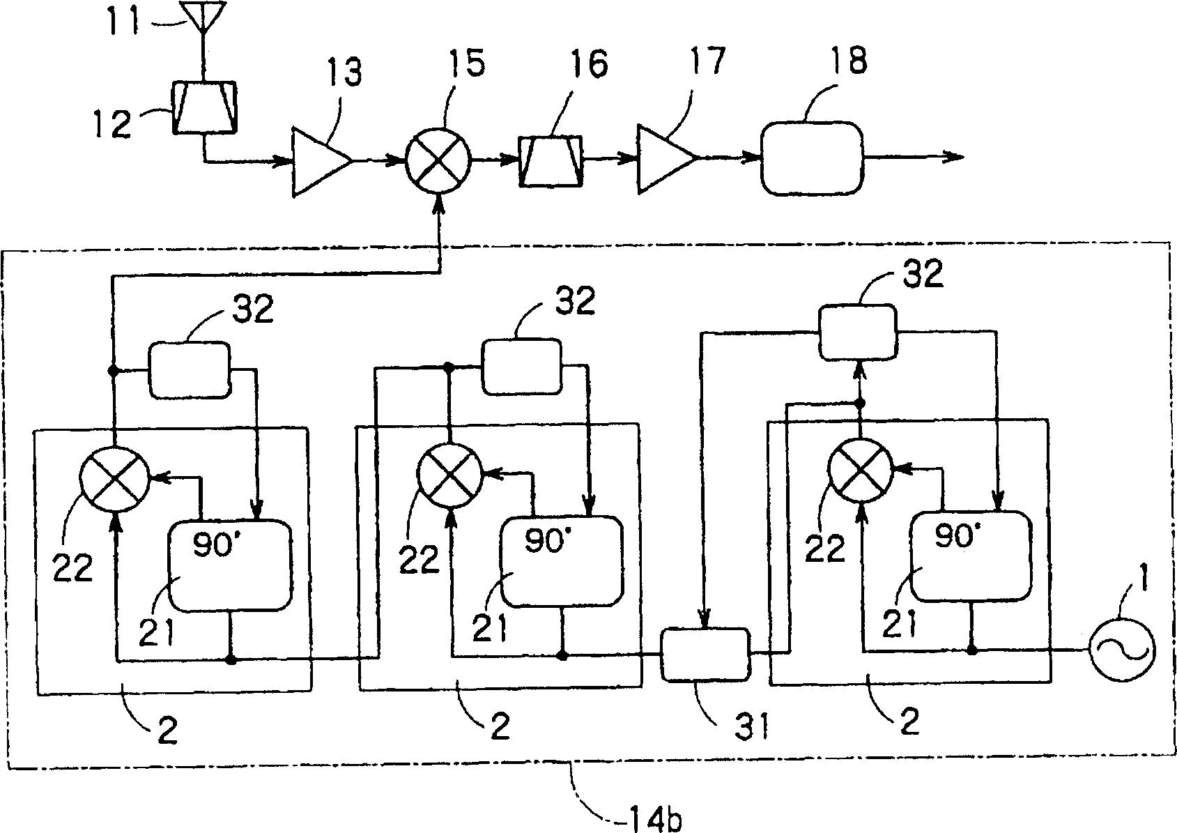
Embodiment 3

[0195] The frequency multiplier circuit of the third embodiment, the configuration of the 90-degree phase shift circuit 21 and the filter circuit 31 are different from those of the second embodiment.

[0196] Figure 6 The circuit diagram shows the detailed configuration of the 90-degree phase shift circuit 21a of the third embodiment. Figure 6 The 90-degree phase shifting circuit 21a is a CR phase-shifting circuit using semiconductor devices (transistors), and its composition is a 45-degree phase shifting part (first and second phase shifting parts) 60-level phase shifting 45 degrees in two stages Link up.

[0197] Figure 6 The 45-degree phase shifting part 60 has transistors Q1 and Q2 for supplying the output of the reference oscillator 41 to the base terminal, connected to the capacitor C5 between the emitter terminals of the transistors Q1 and Q2, and respectively connected to the emitters of the transistors Q1 and Q2. Current sources 61, 62 on the terminals. The current s...


PUM


Abstract

A frequency multiplication circuit with simple structure capable of surely removing unwanted higher harmonics. Inside the oscillation circuit 14a, cascade-connected three stages of 2-multiplication circuits 2 are provided. Since an 8-multiplied local oscillation signal is generated by supplying the source oscillation signal of the crystal oscillator to the 2-multiplication circuit 2 of the first stage, even when a source oscillation frequency is low, the local oscillation signal of a sufficiently high frequency can be generated. By providing a filter circuit 31 between the stages of the frequency multiplication circuit 2, a fixed phase shift quantity generated by a limiter amplifier 26 of the 90 deg. phase shift circuit 21a can be canceled by resistors R6-R8 inserted to the filter circuit 31, so that generation of unwanted higher harmonics is surely suppressed.

Description

Technical field [0001] The present invention relates to a frequency multiplier circuit for generating local oscillator signals used in superheterodyne receivers and the like. Background technique [0002] Recently, many systems have been proposed that transmit and receive weak radio waves and perform various processing in a non-contact manner. For example, a key-less entry system is a system that uses a receiving circuit on the side of the vehicle to receive weak radio waves emitted by a transmitting circuit embedded in the car key to open and close the door. [0003] Figure 15 The block diagram shows the general structure of this existing weak radio wave transmitting and receiving system. Figure 15 The system is roughly divided into a transmitter 51 and a receiver 52. The transmitter 51 has a transmitting circuit 53 and an antenna 54. The transmitter 51 uses 315 MHz as the carrier frequency to transmit AM modulated (amplitude modulation) or FM modulated (frequency modulation)...

Claims


Application Information

Patent Timeline
Patent Type & Authority Patents(China)
IPC IPC(8): H03B19/14H03B21/01H03B21/04
CPCH03B21/01H03B21/04H03B19/14H03C1/00
Inventor 增本博铃木恒雄今山辉男
Owner KK TOSHIBA
Why Eureka
Try Eureka