Supercharge Your Innovation With Domain-Expert AI Agents!

Electronic package for electronic element and manufacturing method thereof

A technology for electronic packaging and conductive parts, applied in the field of organic multi-layer interconnection structures, can solve problems such as increasing the cost of electronic packaging and limiting the electrical performance of organic electronic packaging.

Inactive Publication Date: 2005-01-12
ULTRATECH INT INC
View PDF0 Cites 0 Cited by
  • Summary
  • Abstract
  • Description
  • Claims
  • Application Information

AI Technical Summary

Problems solved by technology

These limitations can limit the superior electrical performance of organic electronic packaging, or significantly increase the cost of electronic packaging

Method used


Image

  • Electronic package for electronic element and manufacturing method thereof
  • Electronic package for electronic element and manufacturing method thereof
  • Electronic package for electronic element and manufacturing method thereof

Examples


Embodiment Construction

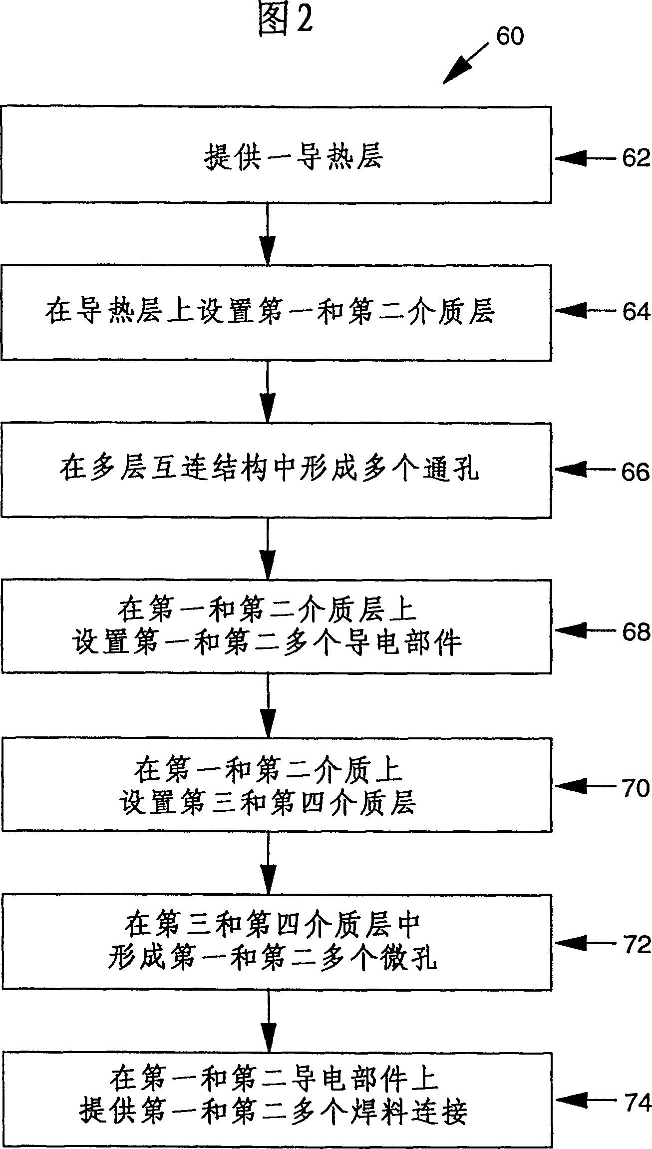
[0022] The present invention provides an electronic package comprising a multilayer interconnection structure (organic chip carrier) and a semiconductor chip, the multilayer interconnection structure is relatively compliant and has a CTE of about 10 to 12 parts per million per degree Celsius, substantially preventing Failure of the interconnect between the semiconductor chip and the printed circuit board on which the package will be assembled.

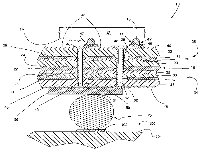
[0023] Referring to FIG. 1 , a front partial cross-sectional view of one embodiment of an electronic package 10 of the present invention is shown. The electronic package 10 includes a semiconductor chip 12 having a first surface 14 including a plurality of contact features 16 thereon. The plurality of contact features are preferably solder balls that control the collapse of the chip connections (C4), each connected to a respective contact (not shown) on the first surface 14 of the chip. Other contact member shapes used in the present ...


PUM

PropertyMeasurementUnit
thicknessaaaaaaaaaa
thicknessaaaaaaaaaa
diameteraaaaaaaaaa

Abstract

A method of making an electronic package. The method includes forming a semiconductor chip and an multi-layered interconnect structure. The semiconductor chip includes a plurality of contact members on one of its surfaces that are connected to the multi-layered interconnect structure by a plurality of solder connections. The formed multi-layered interconnect structure is adapted for electrically interconnecting the semiconductor chip to a circuitized substrate (eg., circuit board) with another plurality of solder connections and includes a thermally conductive layer being comprised of a material having a selected thickness and coefficient of thermal expansion to substantially prevent failure of the solder connections between said first plurality of electrically conductive members and the semiconductor chip. The method forms the electronic package to further include a dielectric material having an effective modulus to assure sufficient compliancy of the multi-layered interconnect structure during operation.

Description

technical field [0001] This invention relates generally to electronic packages for mounting integrated circuits, and more particularly to organic multilayer interconnect structures for use in such packages. Background technique [0002] Organic substrates, such as printed circuit boards and chip carriers, have been and are being developed for many applications. Especially in many chip carrier applications, they are promising replacements for ceramic substrates due to cost reduction and enhanced electrical performance. The use of multilayer interconnect structures such as organic chip carriers to interconnect semiconductor chips to printed circuit boards in electronic packaging introduces many challenges, one of which is the reliability of the connection point between the semiconductor chip and the organic chip carrier, Another is the reliability of the connection point between the organic chip carrier and the printed circuit board. [0003] Since the increase in the number...

Claims


Application Information

Patent Timeline
Patent Type & Authority Patents(China)
IPC IPC(8): H01L23/32H01L23/373H01L23/498H05K1/11H05K3/42H05K3/46
CPCH05K3/429H01L2924/15311H05K3/4602H05K2201/068H05K3/4641H01L2924/3011H01L23/49822H05K2201/09536H05K2201/0191H05K1/114H01L23/3735H01L2224/16225H01L2924/12044H01L2924/00014H01L2924/01322Y10T29/49126Y10T29/4913Y10T29/49144Y10T29/49146Y10T29/49155Y10T29/49165H01L2924/00H01L2224/0401
Inventor 约翰·S·克勒格罗伯特·D·瑟伯斯塔戴维·B·斯通詹姆斯·R·威尔科克斯
Owner ULTRATECH INT INC
Features
  • R&D
  • Intellectual Property
  • Life Sciences
  • Materials
  • Tech Scout
  • Unparalleled Data Quality
  • Higher Quality Content
  • 60% Fewer Hallucinations
Learn More