Luminuous diode packaging structure and its method

A technology of light-emitting diodes and packaging structures, which is applied in the direction of electrical components, circuits, semiconductor devices, etc., and can solve the problem of difficulty in accurately controlling accuracy and uneven color temperature directly above the tube chip and at the junction of the chip and the conical reflector cup, etc. question

Inactive Publication Date: 2005-07-20
IND TECH RES INST
View PDF0 Cites 1 Cited by
  • Summary
  • Abstract
  • Description
  • Claims
  • Application Information

AI Technical Summary

Problems solved by technology

This processing method is also difficult to produce a uniform film, because the specific gravity of the phosphor is much larger than that of the volatile solution, and the precipitation rate of the phosphor is faster than the volatilization rate of the solution
Finally, the phosphor film formed on the surface of the light-emitting diode chip is easy to deposit on the top of the light-emitting diode chip and the junction of the chip and the conical reflective cup, while the phosphor layer on the side without gravity is thinner, which is also unavoidable. The phenomenon of uneven color temperature; on the other hand, the volume of each drop of phosphor solution is about one ten-thousandth of a milliliter, and it is difficult to accurately control the accuracy of each drop of solution volume in the process

Method used


Image

  • Luminuous diode packaging structure and its method
  • Luminuous diode packaging structure and its method
  • Luminuous diode packaging structure and its method

Examples


Embodiment Construction

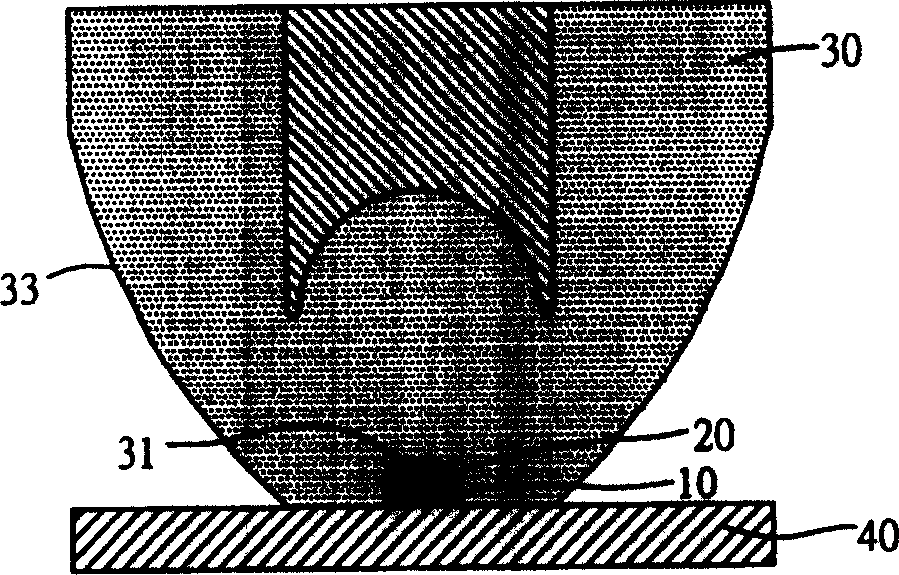
[0021] Please refer to figure 1 , which is a schematic cross-sectional view of a light emitting diode package structure according to an embodiment of the present invention. It includes a light emitting diode 10, a condenser lens 30 and a fluorescent powder adhesive film 20 filled between them. The light-emitting diode connected to the substrate 40 is housed in the cavity 31 of the condenser, and at the same time, there is an appropriate amount of fluorescent powder adhesive film 20 in the cavity 31 to cover the surface of the light-emitting diode 10, and the pre-formed cavity 31 is used to control the fluorescence. The thickness and shape of the powder glue film 20.

[0022] Such as figure 1 As shown, the concentrator 30 of the embodiment of the present invention is a tapered transparent plastic component, which can be made by plastic injection molding. The shape of the diode and the required thickness of the phosphor adhesive film 20 are designed in accordance with the dis...


PUM


Abstract

The packaging structure for luminous diode and fluorescent powder colloid is dropped on pre-shaped depression condenser and setting the luminous diode fixed on base sheet into the depression. At the same time of setting, the surplus of fluorescent powder colloid is extruded out of the expression and fluorescent powder colloid film wrapped on the luminous diode can be finished after the fluorescent powder colloid is form-solidified. The thickness and shape of this film are controlled by pre-shaped depression so uniform colour temperature can be obtained as designed.

Description

technical field [0001] The invention relates to a light emitting diode packaging structure and method thereof, in particular to a light emitting diode packaging structure capable of emitting light with uniform color temperature and a method thereof. Background technique [0002] A light emitting diode (Light Emitting Diode, LED) is a semiconductor light emitting device. Unlike traditional incandescent bulbs, which use a large current to heat up the filament to emit light, a light emitting diode only needs a very small current to stimulate considerable light. Light-emitting diodes use the electrons and holes in semiconductor materials to recombine to display the energy released by emitting light; light-emitting diodes have small size, long life, low driving voltage, low power consumption, fast reaction rate, and shock resistance. Good color and good monochromaticity, etc., are the light-emitting components of various electrical appliances, information boards, communication pr...

Claims


Application Information

Patent Timeline
Patent Type & Authority Patents(China)
IPC IPC(8): H01L33/48H01L33/58
Inventor 韩伟国陈秋伶黄胜邦许荣宗
Owner IND TECH RES INST
Why Eureka
Try Eureka