
Method for producing image-forming apparatus

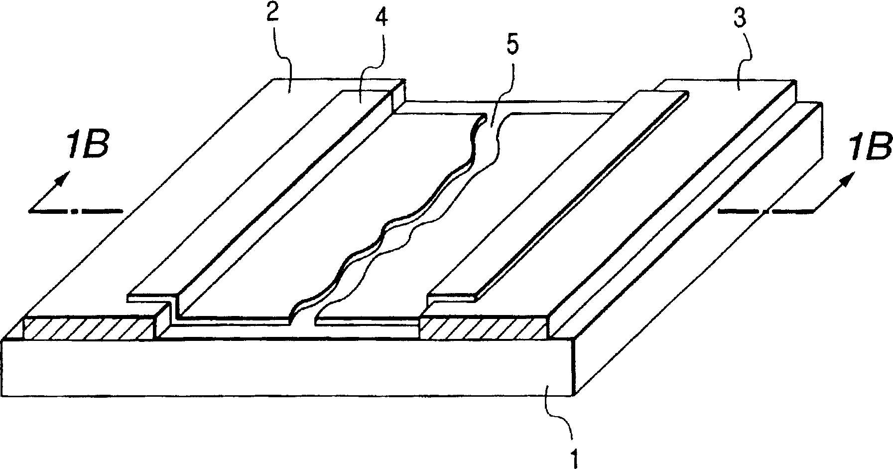
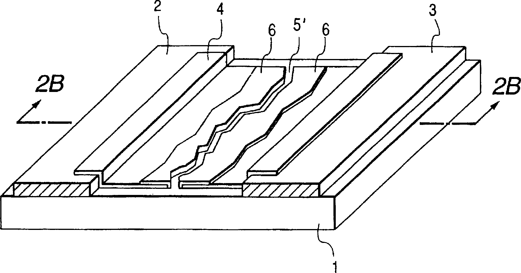
A method for generating images and a technology for image generation, which can be applied in the directions of image/graphic display tubes, image copiers, discharge tubes, etc., and can solve the problems of increased and inappropriate factors restricting the structure of display devices.

Inactive Publication Date: 2005-08-03
CANON KK
View PDF3 Cites 0 Cited by
  • Summary
  • Abstract
  • Description
  • Claims
  • Application Information

AI Technical Summary

Problems solved by technology

However, general drying at hundreds of degrees (°C) is not appropriate, so it cannot be said that this drying is a good solution for the aforementioned problems
As a result of drying at higher temperatures, components that are not resistant to high temperature vacuum drying cannot be used, that is, these components must undergo chemical reactions, alloy compositions, adhered thin films, etc., as well as the components used in display devices. The combination increases the factors restricting the structure of the display device, which is not advisable

Method used


Image

  • Method for producing image-forming apparatus
  • Method for producing image-forming apparatus
  • Method for producing image-forming apparatus

Examples


example 1

[0138] This example is an example of an aging step according to the present invention. In the case of manufacturing an image forming apparatus in which a large number of surface-conduction electron-emitting devices are arranged in a simple matrix layout on an electron source substrate, the aging process is performed by using the manufacturing equipment while the getter is evaporating. and encapsulation performed before.

[0139] Figure 13 is a schematic diagram of an aging apparatus for performing an aging step according to the present invention, for a panel container 101 of an image forming apparatus.

[0140] exist Figure 13 Among them, 101 is a screen container, 121 is an electron source drive control unit, 122 is a data acquisition / analysis unit, 123 is an electron source drive unit, 124 is a drive current measurement unit, 125 is an anode current measurement unit, 126 is a drive signal bus, 127 is the device current bus, and 128 is the transmit current signal bus.

...

example 2

[0184] This example is a manufacturing period of an image forming apparatus in which a large number of surface conduction electron emission devices are arranged in a simple matrix layout on an electron source substrate according to the present invention, by using the image forming apparatus, after the getter evaporation and packaging steps An example of the aging procedure.

[0185] A picture display panel 101 using a large number of surface-conduction electron-emitting devices was fabricated in the same manner as in Example 1. In this example, the materials and dimensions used for the display screen 101 are the same as those in Example 1, except that the x-direction interval between the electron-emitting devices and the phosphor member interval of each color on the panel are 360 ​​μm, however, in the display screen 101 In the generation step, the encapsulation / getter evaporation step performed after the stabilization step does not carry out the aging step.

[0186] the...

example 3

[0200] The image forming apparatus produced in this example has the same structure as the image forming apparatus of Example 2 and all the processing conditions of each step, except for forming operation, energizing operation, stabilizing operation, gettering operation, aging operation, and encapsulation. And outside of the generation step of the image forming apparatus performed after the pumping.

[0201] The image-forming apparatus of this example produced as described above was driven in the same manner as in Example 2, and the emission current Ie therein was measured and compared with that of the Example 2 control. The results are shown in Table 3.

[0202] (μA)

[0203] As can be seen from the table, the image forming apparatus obtained through the aging step of the present invention, compared with the image forming apparatus of the example control object, has formed a high-quality display image (very little deviation) from the start of driving to the...


PUM


Abstract

A method for producing an image-forming apparatus, the image-forming apparatus comprises a container, an electron-emitting device disposed in the container and has an electron-emitting section between a pair of electrodes, the electron-emitting device being adapted to emit electrons with application of a voltage between the pair of electrodes, and an image-forming member for forming an image by irradiation of the electrons emitted from the electron-emitting device, the production method having a step of irradiating the image-forming member with electrons emitted from the electron-emitting device, wherein the electrons to irradiate the image-forming member are electrons emitted by applying to the electron-emitting device the voltage of an opposite polarity to that of a voltage applied between the pair of electrodes of the electron-emitting device during driving for image formation of the image-forming apparatus.

Description

technical field [0001] The present invention relates to a method of producing an image forming apparatus from an electron emission device. Background technique [0002] Generally known electron emission devices are roughly classified into two types using thermionic emission devices and using cold cathode emission devices. Cold cathode emission devices include field emission type (hereinafter referred to as "FE type") devices, metal / insulator / metal type (hereinafter referred to as "MIM type" devices, surface conduction (conduction) electron emission devices, etc. Known Examples including these FE-type devices are disclosed in W.P.Dyke & W.W.Dolan, Introduction to "Field Emission" in Electron Physics, 8, 89 (1956) or in C.A. Spindt, "Physical Properties of Thin Film Field Emission Cathodes with Molybdenum Cones" In, J.Appl.phys., 47, 5248 (1976), etc. Known to comprise the example of these MIM type devices and reveal in C.A.Mead, " in the operation of " tunnel launching devic...

Claims


Application Information

Patent Timeline
IPC IPC(8): H01J31/12
CPCH01J2201/3165H01J31/126
Inventor 浜元康弘
Owner CANON KK
Learn More