
Field effect transistors with improved implants and method for making such transistors

A field-effect transistor, transistor technology, applied in semiconductor/solid-state device manufacturing, electrical solid-state devices, semiconductor devices, etc., to achieve the effect of performance improvement

Inactive Publication Date: 2005-09-14
IBM CORP
View PDF4 Cites 0 Cited by
  • Summary
  • Abstract
  • Description
  • Claims
  • Application Information

AI Technical Summary

Problems solved by technology

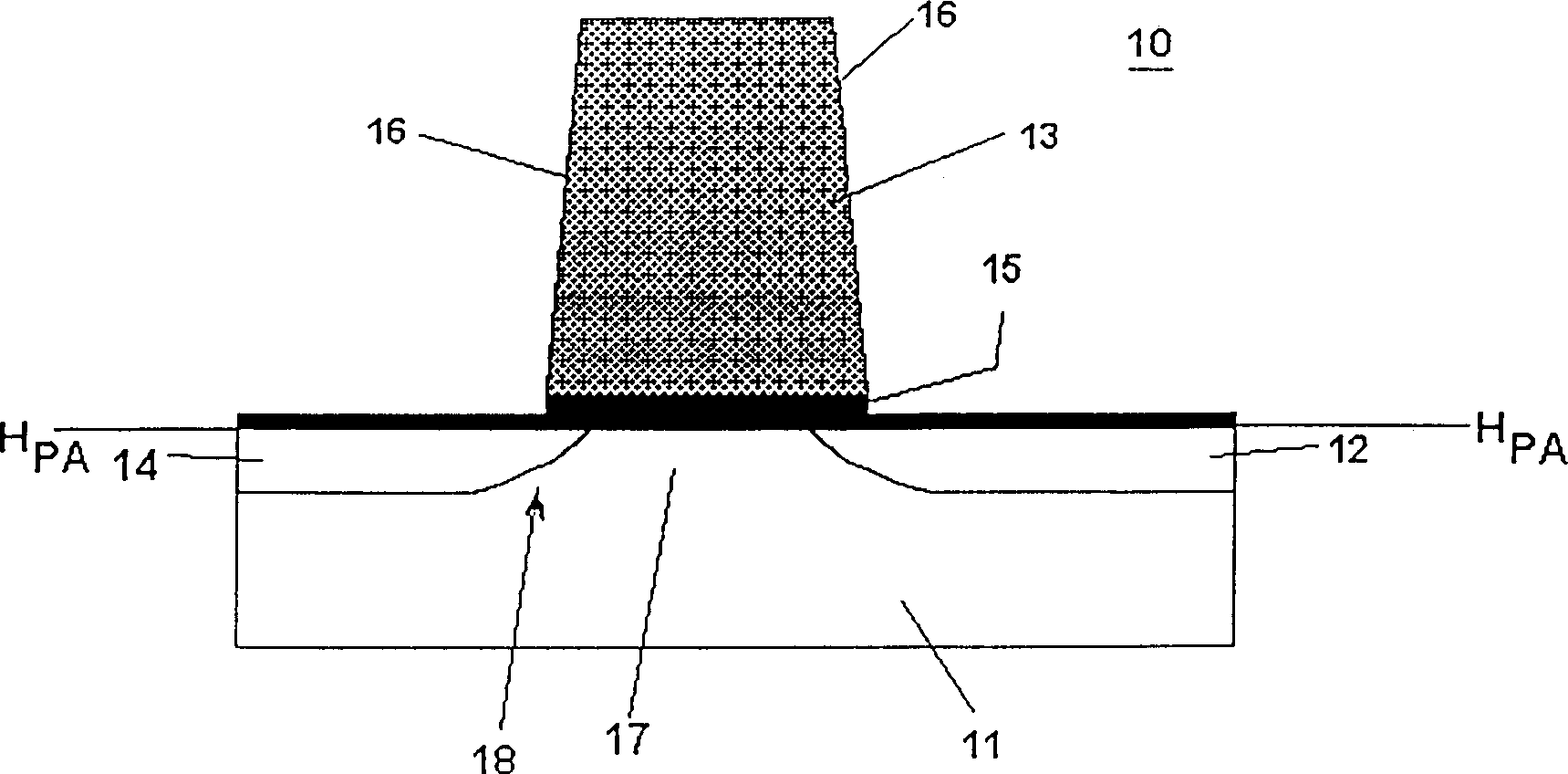
[0008] There is currently no known fabrication scheme for FETs where the threshold-adjust and punch-through implants are well defined and located only below the channel

Method used


Image

  • Field effect transistors with improved implants and method for making such transistors
  • Field effect transistors with improved implants and method for making such transistors
  • Field effect transistors with improved implants and method for making such transistors

Examples


Embodiment Construction

[0053] In this article, n + or p +Doped semiconductor means heavily doped semiconductor. Typically they have at least 10 19 to 10 22 / cm 3 the dopant concentration. The n or p doped region typically has 1×10 17 to 1×10 18 / cm 3 The dopant concentration of n - or p - The doped region has approximately 10 16 / cm 3 the dopant concentration.

[0054] When the word FET is used herein, it means any kind of field effect transistor, including MOSFET, CMOS FET, NMOS, PMOS, and the like.

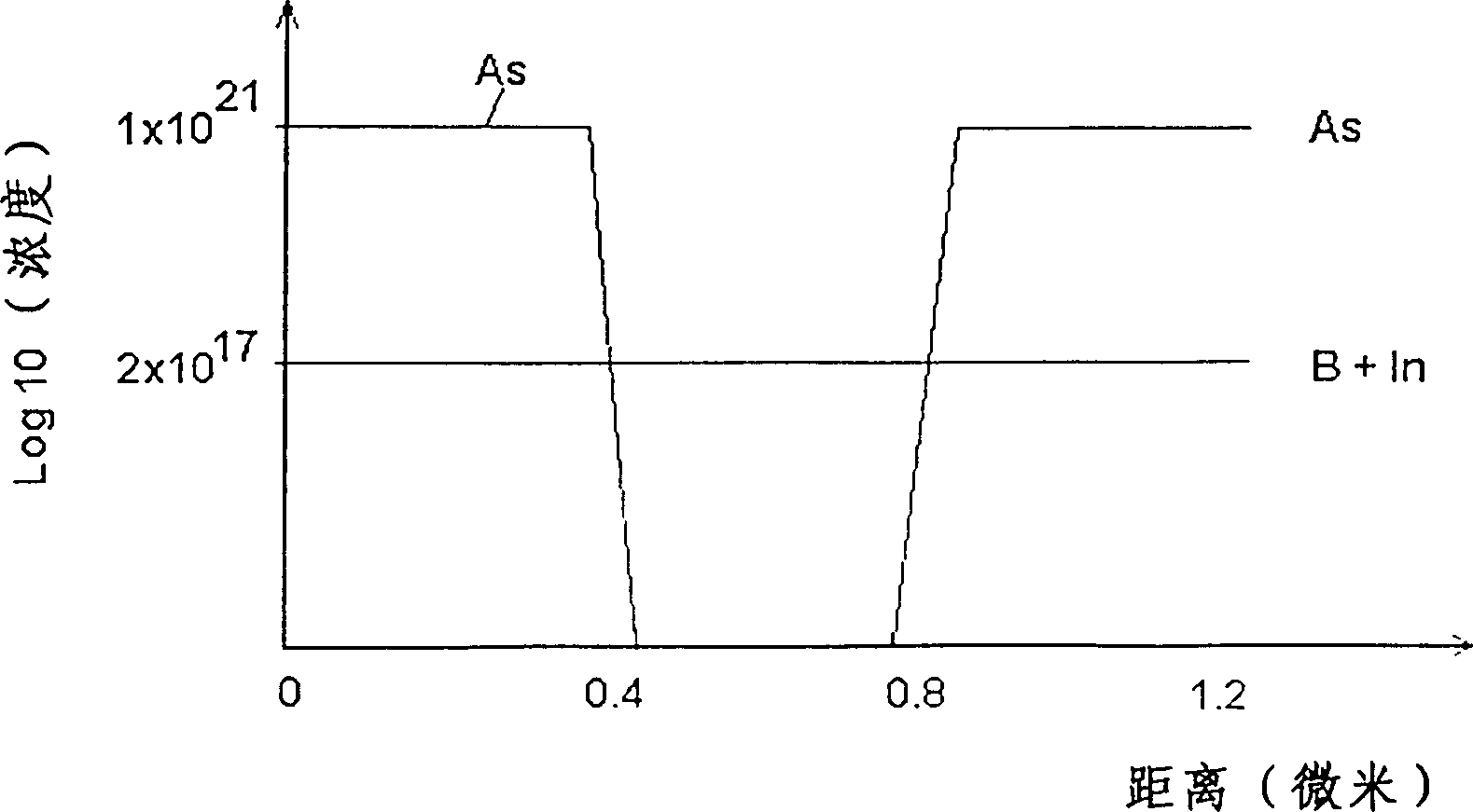
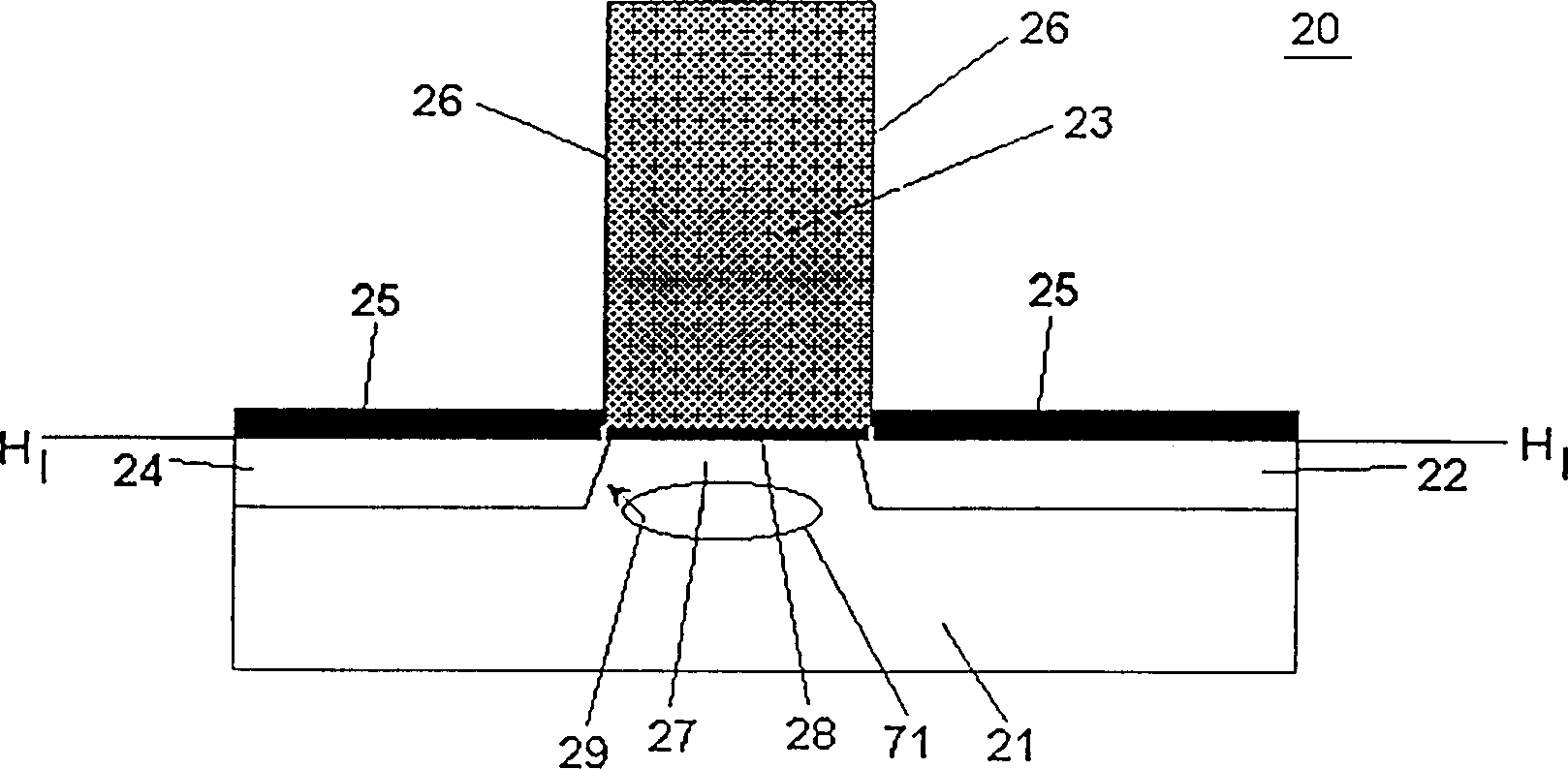
[0055] exist Figure 2A A FET 20 according to the present invention is illustrated in . It is formed in the semiconductor substrate 21 . The substrate may be, for example, a silicon substrate. In this example, by n + Doped to define drain region 22 and source region 24 . Impurities well suited for n-type doping are, for example: P, As and Sb. As is used as a dopant in this embodiment. For defining p-type source and drain regions, B, In and Ga can be used. The polysilicon gate 23 si...


PUM

PropertyMeasurementUnit
Thicknessaaaaaaaaaa
Thicknessaaaaaaaaaa

Abstract

The MOSFET further includes a threshold adjust implant region and / or punch through implant region being aligned with respect to the gate conductor and limited to an area underneath the gate conductor. Such a MOSFET can be made using the following method: forming a dielectric stack on a semiconductor structure; defining an etch window on the dielectric stack having the lateral size and shape of a gate hole to be formed; defining the gate hole in the dielectric stack by transferring the etch window into the dielectric stack using a reactive ion etching (RIE) process; implanting threshold adjust dopants and / or punch through dopants through the gate hole; depositing a gate conductor such that it fills the gate hole; removing the gate conductor covering portions of the semiconductor structure surrounding the gate hole; and removing at least part of the dielectric stack.

Description

technical field [0001] This invention relates generally to metal-oxide-semiconductor field effect transistors (MOSFETs) and, more particularly, to methods of fabricating MOSFETs with improved implants. Background technique [0002] Field effect transistors (FETs) are the basic building blocks of current integrated circuits. Such transistors may be formed in conventional substrates such as silicon substrates or silicon-on-insulator substrates. In both cases, so-called deep implants are introduced into the substrate to improve transistor performance in order to provide heavily doped isolation for complementary metal-oxide (CMOS) integrated circuits, reducing parasitic vertical transistor current gain , and to reduce parasitic latch-up effects, just to mention some of the reasons why deep implants are used. [0003] In CMOS technology, these deep implants are called p-well or n-well deep implants. These p-well or n-well deep implants are required if NMOS transistors (p-well)...

Claims


Application Information

Patent Timeline
IPC IPC(8): H01L21/76H01L21/336H01L21/762H01L21/8234H01L27/08H01L29/78
CPCH01L29/66537H01L21/823481H01L21/823412H01L21/76224H01L29/66583
Inventor 迪亚尼·C·伯伊德斯图亚特·M·伯恩斯侯塞因·I·哈纳非袁·陶尔威廉·C·维尔
Owner IBM CORP
Learn More