Transistor vibrator assembly and its mfg. method, and method for mfg. various connected glass plate used for electronic element assembly
A crystal vibrator and manufacturing method technology, applied in the direction of electrical components, power oscillators, impedance networks, etc., can solve the problems of low productivity, difficulty in miniaturization, and inability to adjust, etc., achieve less wiring, reduce working hours, and increase production. Effect
Inactive Publication Date: 2006-05-10
NIPPON SHEET GLASS CO LTD
1 Cites 0 Cited by
AI-Extracted Technical Summary
Problems solved by technology
[0007] ①Because the crystal plate 12 cannot be observed from the outside after the cover 13 is put on, it is impossible to adjust the frequency characteristics of the crystal plate 12
[0009] 2. Because the crystal vibrator assembly 15 of ...
Method used
The base and the lid covered thereon are all made of glass, and the coefficients of linear expansion of the two are the same, so when the humidity changes, the shell will not be deformed, therefore, the shell can smoothly expand or contract.
The base used by the electronic component assembly is made of material glass with several conjoined stamping methods, and the necessary through holes are processed while stamping, so that in one process conjoined stamping process, it can be obtained (m×n) bases, so the productivity can be increased exceptionally.
The crystal vibrator is directly lapped on the front end face of the protruding end of the metal part, so the electrode used for connecting the crystal can be saved, which not only reduces man-hours, but also reduces manufacturing costs and reduces the cost of finished products .
[0081] Therefore, the present invention that changes the material of the base from ceramics to glass can realize stable vibration performance of the crystal vibrator 14.
[0131] After installing one end of the crystal vibrator 14 on the electrode 13 connected to the crystal, it is advisable to increase the bonding strength through the adhesive 59. Furthermore, since the cover 16 is made of glass and the metal film 56 can be irradiated with the laser beam 56, the frequency of the crystal resonator 14 can be easily adjusted. The symbols of other configurations are not changed, so descriptions are omitted.
[0148] The crystal vibrator assembly of the present invention consists of a base, a crystal vibrator mounted on the base and a cover for closing the crystal vibrator on the base, wherein at least the base and the cover are One is a molding made of glass. That is, in the prior art, the base and/or the cover are made of ceramics, but in the present invention, the moldings are made of glass. Compared with ceramics, glass is not only very easy to form but also has low manufacturing cost. Because glass has low thermal conductivity and good heat insulation, it can play a good role in...
Abstract
The invention provides a crystal vibrator assembly, which consists of a base, a crystal vibrator installed on the base, and a cover for sealing the crystal vibrator on the base, wherein at least one of the base and the cover is made of glass The finished molded product; on one surface of the above-mentioned base, an electrode for connecting the crystal is provided, and on the other surface of the above-mentioned base, an electrode for connecting the outside is provided, and these electrodes for connecting the crystal and the electrode for connecting the outside The electrodes used are electrically connected through the conductive parts buried in the through holes, and the above-mentioned crystal oscillator is lapped on the above-mentioned electrodes for connecting the crystal. The invention also provides a manufacturing method of the crystal vibrator assembly, which is characterized in that it includes the following procedures: forming process; electrode forming process; crystal lapping process; sealing process; cutting process.
Application Domain
Impedence networksOscillations generators
Technology Topic
Electrically conductiveEngineering +7
Image
Examples
- Experimental program(1)
Example Embodiment
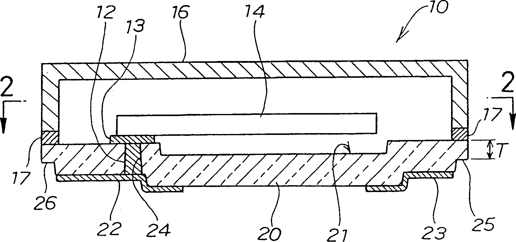
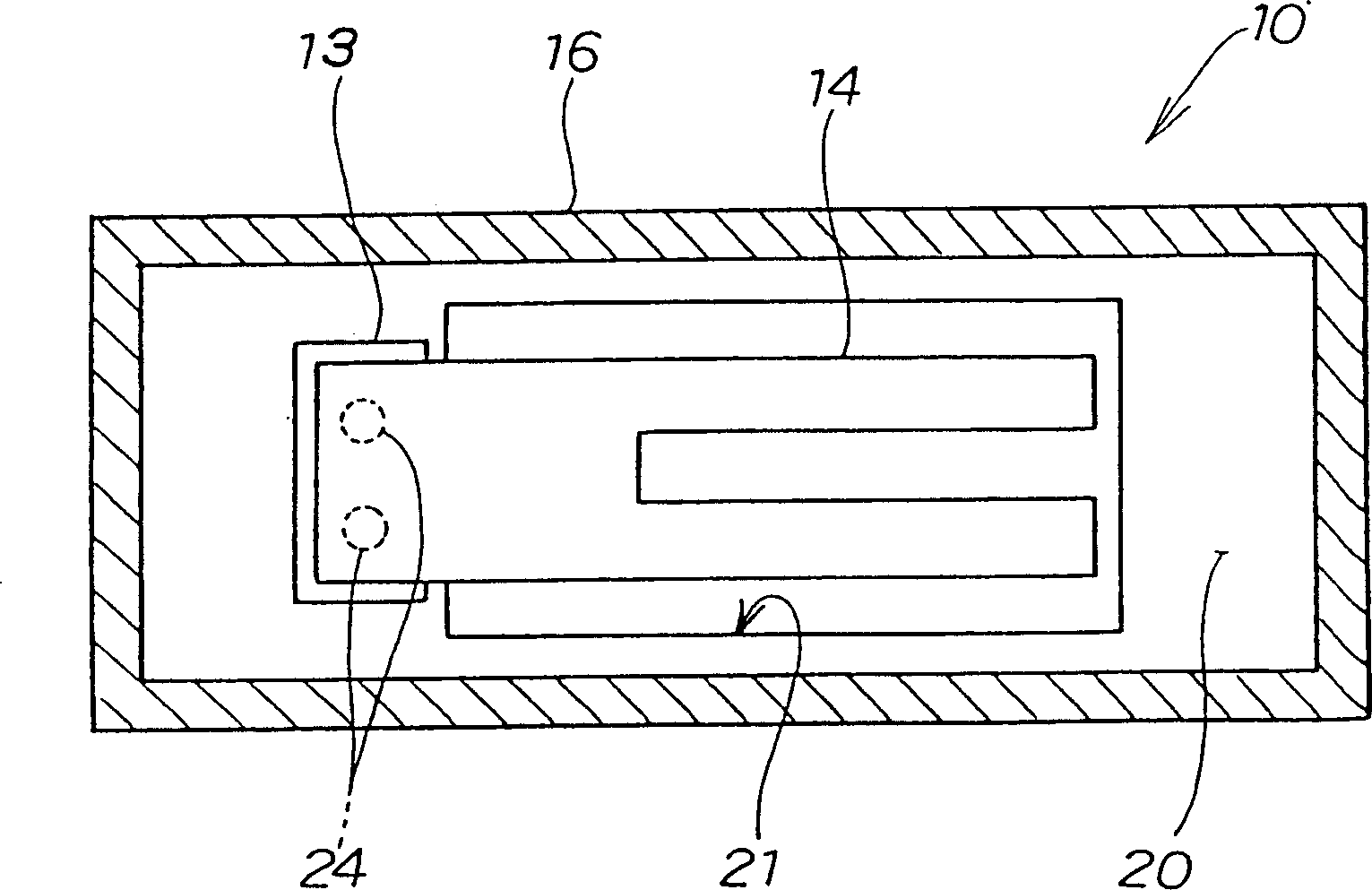
[0075] figure 1 It is a cross-sectional view of the crystal oscillator assembly of the present invention. The crystal oscillator assembly 10 is composed of a base 20 made of glass with high transmittance, and an electrode 13 for connecting the crystal to the base 20 is bonded and installed in a cantilever support state. The crystal oscillator 14 and the cover 16 on the base 20 for closing the crystal oscillator 14 are composed. Among them, 17 is a glass-based adhesive. In order to improve the adhesive force, the edge of the base 20 for applying the glass-based adhesive 17 should be processed to have a surface roughness of 3 to 4 μm. Grinding with alumina abrasives can easily form the rough surface.
[0076] The cover 16 can be made of opaque materials such as metal, but in order to adjust the frequency of the internal crystal oscillator, the laser beam must pass through the base to irradiate the crystal oscillator. Therefore, in order to allow the laser beam to be fully transmitted, it is required to The iron content of the glass plate for manufacturing the base is below 3000 ppm. As a material glass plate-soda lime silicate glass for building doors and windows, alkali-free glass for liquid crystal display and low-alkali glass for PDP display glass, etc. can be used, as long as the transmittance can be ensured, any choice The ingredients are fine.
[0077] The cover 16 can also be a finished product made of transparent glass or made of glass. In this case, at least one surface must be covered with a metal film for electromagnetic sealing. The metal film is connected to the GND (ground) terminal of the base 20 (not shown in the figure), so that the incident of electromagnetic interference from the outside can be blocked, and electromagnetic obstacle noise (EMI noise) emitted from the crystal oscillator can also be blocked. ) The partition is not transmitted to the outside.
[0078] The base and the cover covering it are made of glass. The linear expansion rate of the two is the same. Therefore, when the humidity changes, the shell will not be deformed. Therefore, the shell can expand smoothly or shrink.
[0079] In addition, a recess 21 is provided on the upper surface of the base 20, electrodes 22 and 23 are provided on the lower surface, and through holes 24 are provided on the upper and lower surfaces of the base 20, and the thickness T of the edge 25 is less than 0.3 mm. 12 is a conductive part such as silver paste buried in the through hole 24.
[0080] In the prior art, the base is made of ceramic materials, the thermal conductivity of ceramic is 24.3W/(m·k), and the thermal conductivity of glass is 1W/(m·K). Taking the crystal oscillator assembly 10 built in a mobile phone as an example, when the temperature of exposure to sunlight changes greatly, the heat insulation performance of the base 20 made of glass is more than 20 times higher than that of ceramics. Therefore, the crystal oscillator assembly made of glass When subjected to temperature changes, the crystal oscillator 14 installed therein can also work for a sufficient time.
[0081] Therefore, the present invention in which the material of the base is changed from ceramic to glass can achieve stable vibration performance of the crystal oscillator 14.
[0082] figure 2 Yes figure 1 In the cross-sectional view at center 2-2, when the crystal oscillator assembly 10 is viewed from above, the U-shaped crystal oscillator 14 is supported on the electrode 13 for connecting the crystal and is a cantilever beam extended on the recess 21. Since the crystal oscillator 14 and the recess 21 are surrounded by the cover 16, it shows a structure in which the crystal oscillator is isolated from the outside atmosphere.
[0083] The following describes in order the base 20 made of glass having the above structure, a molding die suitable for manufacturing the base 20 and a manufacturing method using the molding die.
[0084] image 3 It is a schematic diagram of the forming mold for manufacturing the base of the present invention. The forming mold 30 is composed of a movable upper mold 31 and a fixed lower mold 41. The upper mold 31 may also be a fixed type, and the lower mold may be movable.
[0085] In the example, the upper mold 31 is provided with pins 32 for forming through holes... (...representing several, the same below) and protruding portions 33 for forming junctions are provided on the lower mold 41. The lower mold 41 is also provided with recesses for the pins 32 42..., vent hole 43... and convex portion 44... for forming recesses. The material glass is indicated by a dotted line 45.
[0086] That is, the forming die 30 can produce several bases 20 in one stamping process (see figure 1 , 2 ) Of several Siamese models.
[0087] Figure 4 Yes image 3 In the working drawing, several conjoined glass plate bases 50 are obtained by stamping. In the process of lowering the upper mold 31 to the bottom dead center, the through-holes 24... are formed on the several conjoined glass plate bases 50 with the through-hole forming pins 32... and the convex parts 33... which form the junctions are used to form thin At the junction, the concave portion 21... is formed by the convex portion 44... which forms the concave portion.
[0088] The following figure is summarized in Figure 4 Describes the manufacturing method of manufacturing several pedestals of conjoined glass plates.
[0089] Figure 5 It is a process diagram of manufacturing a number of conjoined glass plate bases of the present invention. STXX represents the process number (the same applies below).
[0090] ST01: First, prepare the material glass and forming mold.
[0091] ST02: Put the material glass between the upper and lower molds.
[0092] ST03: Heat the material glass to above its softening point temperature.
[0093] ST04: Implement press forming. Through this punching, a through hole and a thin-walled part are processed at the same time.
[0094] ST05: Send out a number of formed conjoined glass plate bases.
[0095] Figure 6 It is a plan view of several conjoined glass plate bases of the present invention. The several conjoined glass plate bases 50 are provided with recesses 20... and through holes 24... and thin-walled parts 51 at the junction. A checkerboard-like or chocolate-like arrangement of m×n vertical pedestals formed by the vertical thin-walled portion 51 and the horizontal thin-walled portion 51 constitutes a plurality of connected glass plate pedestals 50.
[0096] Hereinafter, a technique of manufacturing a plurality of crystal oscillator assemblies using such a plurality of conjoined glass plate bases 50 will be described.
[0097] Figure 7 (A) to (c) are the first of the manufacturing explanatory diagrams of the crystal unit of the present invention.
[0098] (a) shows a number of conjoined glass plate bases 50 formed by the previous step (ST05), which have recesses 21..., through holes 24... and groove-shaped thin-walled parts 51... .
[0099] (b) shows the assembling process: fill conductive parts 12 such as silver glue into the through holes 24..., and print on the upper and lower surfaces of the one-piece glass plate base 50 for connecting crystals. The electrodes 13... and the electrodes 22..., 23... for connecting to the outside, and the crystal oscillator 14... is bonded to the electrodes 13... for connecting the crystal.
[0100] (c) shows the assembly process in which the cover 16... is glued to the upper surface of the thin-walled portion 51... with a glass-based adhesive 17...
[0101] Figure 8 (A) to (c) are the second of the manufacturing explanatory diagrams of the crystal unit of the present invention.
[0102] (a) Cut the thin-walled part 51... which constitutes the junction with the laser beam 52... for cutting. It is also possible to apply a mechanical bending force to the thin-walled portion 51... and cut it mechanically like pancakes and chocolate.
[0103] As a prerequisite for cutting, the thin-walled portion 51 is processed to be thinner than other portions. Specifically, the thickness of the thin thin-walled portion 51 cannot exceed 0.3 mm. Especially glass is very easy to cut when its thickness is less than 0.3mm. Even if it is cut with a laser beam, the thinner the better.
[0104] Next, (b) the laser beam 53 from the outside of the base 20 passes through the base 20 to focus on the tip of the crystal oscillator 14 to vaporize the tip of the crystal oscillator 14, and the amount of reduction is ΔL, thereby realizing the alignment of the crystal oscillator 14 The frequency adjustment. Therefore, the reserved length of the crystal oscillator 14 should be (L+ΔL), that is, make it longer.
[0105] Since the laser beam 53 is a kind of YAG (yttrium aluminum garnet) laser light, the iron content in the glass has a shielding effect on it, so glass with an iron content of less than 3000 ppm should be used.
[0106] In addition, when a laser is used to irradiate and focus the front end of the crystal oscillator 14 to heat and vaporize the crystal, the crystal oscillator 14 is preferably not in contact with or close to the base 20. If touched or approached, heat will be transferred from the crystal vibrator 14 to the base 20, which will cause difficulties for the part to be vaporized. Also, do not aim at the front end of the crystal oscillator 14 from the side of the base 20.
[0107] There, at least the gap d between the base 20 and the crystal oscillator 14 is 50 μm. The gap d is ensured by the depth of the recess 21 set in the base 20 to have an appropriate depth.
[0108] (c) is a view of another embodiment of (b), that is, the metal film 54 is partially reserved on the crystal oscillator 14. The weight of the metal film 54 can function as a weight. Since the cover 16 is made of glass and light can pass through, the metal film 54 is irradiated with a laser beam 56 from above, and a part of the metal film 54 is vaporized with the heat energy of the laser. As a result, the frequency of the crystal oscillator 14 also changes due to the change in weight. That is, with the method (c), the frequency can be adjusted without shearing the crystal oscillator 14. Depending on the type of crystal resonator, since the metal film 54 is not provided in the front part of the crystal resonator but at the center, the laser beam 54 matches the position of the metal film 54 and is irradiated appropriately.
[0109] use Figure 7 , 8 The described manufacturing method of the crystal oscillator assembly is summarized in Figure 9.
[0110] Picture 9 It is a manufacturing process diagram of the crystal oscillator assembly of the present invention.
[0111] ST11: First, prepare a number of connected glass plate bases (see Figure 7 (a)).
[0112] ST12: Buried silver paste as a conductive material in the through hole (see Figure 7 (b)).
[0113] ST13: Printed electrodes. Gold-plated as needed (see Figure 7 (b)).
[0114] ST14: Install crystal oscillator (see Figure 7 (b)).
[0115] ST15: Installation cover (see Figure 7 (c)).
[0116] ST16: Use laser beam or diamond grinding wheel to cut off the conjoined base or cut off the conjoined base by hand or mechanical breaking. The diamond grinding wheel is formed by adhering diamond grit to the outer circumference of the disc, so the glass can be cut when the disc rotates at high speed.
[0117] ST17: Adjust the frequency of the crystal oscillator with a laser beam (see Figure 8 (b) or (c)).
[0118] ST18: It can be used to obtain crystal oscillator components (see figure 1 , 2 ).
[0119] Picture 10 Yes Picture 9 The improved embodiment diagram, the difference is that Picture 9 The ST18 in the middle is adjusted to the front of ST16 (or ST17). The description will be given below.
[0120] ST21: First, prepare a number of conjoined glass plate bases (see Figure 7 (a)).
[0121] ST22: Buried silver paste as a conductive material in the through hole (see Figure 7 (b)).
[0122] ST23: Printed electrodes, gold-plated as required (see Figure 7 (b)).
[0123] ST24: Install crystal oscillator (see Figure 7 (b)).
[0124] ST25: Installation cover (see Figure 7 (c)).
[0125] ST26: Adjust the crystal oscillator frequency with a laser beam (see Figure 8 (b) or (c)).
[0126] ST27: Use laser beam or diamond grinding wheel to cut off the conjoined base or cut off the conjoined base by hand or mechanical breaking.
[0127] ST28: It can be used to obtain crystal oscillator components (see figure 1 , 2 ).
[0128] Picture 11 Yes figure 1 The improved embodiment diagram of the crystal oscillator assembly 10 is made of a base 20 made of glass with high transmittance, a crystal oscillator 14 which is connected to the electrode 13 for connecting the crystal on the base 20 and supported in a cantilever manner, and is used for The cover 16 covering the base 20 for closing the crystal oscillator 14 is composed of a base protection plate 55 made of glass adhered to the bottom of the base 20.
[0129] The base protection plate 55 can play a sealing function, that is, it can cut off the leakage through the through hole 24 or effectively prevent the intrusion of the atmosphere.
[0130] Picture 12 Yes figure 1 Another improved embodiment diagram of the crystal oscillator assembly 10 is characterized in that electrodes 22 and 23 for connecting to the outside are provided on one surface of the base 20. On the other surface of the base 20, an electrode 13 for connecting the crystal is provided, and the crystal oscillator 14 is overlapped on the electrode 13 for connecting the crystal. At the same time, a metal part 58 penetrating the base 20 is used to connect the external The electrode 22 and the electrode 14 for connecting the crystal are connected with current.
[0131] After mounting one end of the crystal oscillator 14 on the electrode 13 connected to the crystal, it is better to use an adhesive 59 to increase the bonding strength. In addition, the cover 16 is a finished product made of glass, and the metal film 56 can be irradiated with the laser beam 56. Therefore, the frequency of the crystal oscillator 14 can be easily adjusted. The symbols of the other components remain unchanged, so the description is omitted.
[0132] Figure 13 Yes Picture 12 In the cross-sectional view at 13-15, the crystal oscillator 14 is overlapped on the electrodes 13 and 13 for connecting the crystal, and metal parts 58, 58 are connected under the electrodes 13 and 13 for connecting the crystal.
[0133] Picture 14 Yes Picture 12 The 14-14 views of the base 20 are printed on one surface of the base 20 to form electrodes 22, 22, 23, 23 for connecting to the outside, and metal parts 58, 58 to the electrodes 22, 22 for connecting to the outside The inner surface extends.
[0134] Figure 15 (a)~(c) shows Picture 12 The main points of the installation of metal parts.
[0135] For example, in (a), a small-diameter through hole 61 is opened in the base 20, and a pin-shaped metal part 58 is driven into the through hole 61 while the base 20 is in a thermally softened state.
[0136] (b) shows the metal part 58 and the base 20 after driving.
[0137] In (c), the external electrodes 22 and 23 are printed on one surface of the base 20, and the electrode 13 for connecting the crystal is printed on the other surface. The crystal oscillator 14 can be mounted on the connecting crystal. Used electrode 13 on.
[0138] Figure 16 (a)~(d) are Figure 15 The improved embodiment diagram.
[0139] In (a), a metal part 62 of a special shape is pressed into the base 20.
[0140] (b) is a perspective view of a special-shaped metal part 62, (c) is a cross-sectional view at cc of (a), the metal part 62 is a flat head composed of a large flat head 63 and a rectangular cross-section shaft 64 pin.
[0141] In (d), the crystal oscillator 14 is directly adhered to the flat head 63 of the metal part 62 with an adhesive 63. This saves the electrode 13 for connecting the crystal (see Figure 15 (C)).
[0142] Figure 17 Yes figure 1 In another improved embodiment diagram, in the crystal oscillator assembly 10, thick pin-shaped metal parts 66, 67 are pressed into the base 20, and one end of the metal parts 66, 67 (the lower end in the figure) is connected to The external electrodes 22 and 23 are connected, the crystal oscillator 14 is attached to the metal parts 66 and 67, and the one metal part 66 is fixed with an adhesive 59.
[0143] Figure 18 Yes Figure 17 In the cross-sectional view at the center 18-18, the crystal oscillator 14 is mounted on the metal parts 66, 66, 67. The symbols of the other components remain unchanged, so the description is omitted.
[0144] Figure 19 Yes figure 1 The improved embodiment diagram, and figure 1 The same part figure 1 The description is omitted. That is, in the crystal unit 10, the cover is integrally formed by bonding the four walls 69 to the flat plate 68 with the adhesive 17. In this way, the crystal oscillator assembly 10 is formed by stacking the three elements of the base 20, the four walls 69 and the flat plate 68. The tablet 68 is easy to manufacture and inexpensive. The same is true for Sibi 69. Therefore, the cost of the crystal unit 10 can be reduced.
[0145] Picture 20 Yes figure 1 In another improved embodiment diagram, the electrodes 22 and 23 for external connection extend to the side and upper surface of the base 20. In addition, the crystal oscillator 14 is directly connected to the electrode 22 for connecting to the outside. This can save figure 1 In the conductive parts 12 and the electrode 13.
[0146] The several conjoined glass plate bases manufactured by the method of the present invention are very suitable for mounting a crystal oscillator on the base, and it is also suitable for mounting other solid circuit combination components such as transistors and diodes. Therefore, a number of conjoined glass plate bases manufactured by the above method can be widely used in the manufacture of electronic component assemblies.
[0147] With the above structure of the present invention, the following effects can be exerted:
[0148] The crystal oscillator assembly of the present invention is composed of a base, a crystal oscillator mounted on the base, and a cover for closing the crystal oscillator on the base. It is characterized in that at least one of the base and the cover is used Molded products made of glass. That is, in the prior art, the base and/or the cover are made of ceramics, while the present invention is a molded article made of glass. Compared with ceramics, glass is not only very easy to shape, but also has low manufacturing cost. Because glass has low thermal conductivity and good thermal insulation, it can play a good role in protecting the internal crystal oscillator. In addition, since the base and/or cover are made of a glass plate with a high transmission coefficient, it is possible to easily adjust the frequency characteristics of the built-in crystal oscillator with a laser beam.
[0149] A gap of at least 50 μm is provided between the base and the crystal oscillator.
[0150] Since the above-mentioned gap is provided, it is easy to cut only the crystal oscillator with a laser beam. The gap is less than 50 μm, and the heat applied to the crystal oscillator is transferred to the base, which not only reduces the workability, but may also cause the base to melt. Therefore, a gap of at least 50 μm must be provided between the base and the crystal oscillator.
[0151] In order to ensure the above gap, a recess is provided on the base.
[0152] In order to ensure the gap, although several structures are considered, the simple structure is to provide a recess on the base, which can reduce the manufacturing cost.
[0153] At least the outer surface of the cover is covered with an electromagnetic shielding film.
[0154] This can cut off the electromagnetic interference from the outside or cut off the noise from the electromagnetic failure of the crystal oscillator.
[0155] An electrode for connecting to the crystal is provided on one surface of the base, and an electrode for connecting to the outside is provided on the other surface of the base, and these electrodes for connecting to the crystal and the electrode for connecting to the outside are buried The conductive part in the through hole is connected to the current, and the crystal oscillator is overlapped on the electrode for connecting the crystal.
[0156] Since the electrode for connecting the crystal and the electrode for connecting to the outside are directly connected through the through hole, the amount of wiring is small, and the electrical characteristics of the crystal oscillator are stable.
[0157] An electrode for connecting to the outside is provided on one surface of the base, an electrode for connecting to the crystal is provided on the other surface of the base, the crystal oscillator is overlapped on the electrode for connecting to the crystal, and a penetrating The metal parts of the base connect the electrodes for connecting the external and the electrodes for connecting the crystal with current.
[0158] Due to the good conductivity of metal parts, the electrical characteristics of the crystal oscillator can be more stable.
[0159] An electrode for connecting to the outside is provided on one surface of the base, the electrode for connecting to the outside is connected with a metal part penetrating the base, and the metal part extends from the other surface of the base iron, The above-mentioned crystal oscillator is directly overlapped on the front end surface of the protruding part.
[0160] The crystal oscillator is directly connected to the front end surface of the extension end of the metal part from the ground, so the electrode for connecting the crystal can be omitted, which not only reduces man-hours, but also reduces the manufacturing cost and the cost of the finished product.
[0161] The method for manufacturing a crystal oscillator assembly provided by the present invention is characterized by including the following procedures:
[0162] The forming process, that is, the material glass is placed between the upper and lower molds of the forming mold, the material glass is heated to a temperature above its softening point, and a glass plate is press-formed, and the above-mentioned glass plate is press-formed in length m×width n Several conjoined bases for each crystal oscillator component;
[0163] The electrode formation step is to provide conductive parts from one surface to the other of the obtained substrates, and to form on each of the above-mentioned conductive parts an electrode for connecting to the outside and a crystal connecting electrode. electrode;
[0164] Crystal lap process, that is, lap the crystal oscillator on the electrode for connecting the crystal;
[0165] The sealing process is to close the crystal oscillator and cover the base on the base;
[0166] The cutting process is to cut the above-mentioned one glass plate into m×n crystal oscillator assemblies using the above-mentioned base as a unit.
[0167] Since the base of the module is made of material glass according to several one-piece punching methods, the one-piece type is adopted, and (m×n) bases can be obtained by one punching, so the productivity can be increased significantly. .
[0168] Since the crystal oscillator is installed on a glass plate formed by several conjoined bases, the cover is placed on the base, and then the base is divided to obtain m×n crystal oscillator components, so the crystal oscillator can be improved The production volume of the component.
[0169] In addition, since the crystal oscillator and the cover are mounted in the state of a so-called large glass plate and then divided, the size of the crystal oscillator assembly can be easily achieved.
[0170] Before or after the cutting process, use a laser beam from the outside of the housing through the base to irradiate and focus on the crystal oscillator to vaporize a part of the crystal oscillator, or remove a part of the metal film covering the crystal oscillator, thereby realizing the control of the crystal oscillator Frequency adjustment.
[0171] Since the base is made of glass with high transmission coefficient, the frequency of the crystal oscillator can be adjusted after assembly. Therefore, the frequency characteristics of the crystal unit can be controlled with high accuracy.
[0172] The cutting in the above-mentioned cutting process can be fused with a laser beam, ground with a diamond grinding wheel, or mechanically bent and cut.
[0173] Cutting with a laser beam can shorten the time required for cutting or mechanical cutting can be done with an inexpensive bending machine, but the output is small and it can also be broken manually. Therefore, the production cost can be reduced.
[0174] In the above-mentioned forming process, at the same time of forming, a pin provided on the forming mold is used to form a through hole that penetrates one surface to the other surface of the base in the base.
[0175] Because the pin is provided on the forming mold, the through hole can be formed in the forming process. In conventional technology, the forming process and the through hole processing process are performed separately. The present invention combines the above two processes into one process It is very economical, which reduces the processing steps.
[0176] In the electrode forming step, the conductive component is buried in the through hole of the base, and at the same time, an electrode for connecting to the outside and an electrode for connecting to the crystal are formed on the base by a printing method.
[0177] The printing method can form efficient electrodes in a short time. That is, according to the present invention, the electrode forming time in the electrode forming process can be shortened, and therefore the process time for manufacturing the crystal oscillator assembly can be shortened.
[0178] The base used for the electronic component assembly is made of material glass with several one-piece punching methods, and the necessary through holes are processed at the same time during the punching, so that the one-piece punching process can be obtained (m× n) bases, so productivity can be improved exceptionally.
[0179] While heating the material glass to above its softening point temperature, the junction of adjacent susceptors is processed to be thinner than other parts. Since the junction between the base and the base is processed to be thinner than other parts, it is easy to realize the subsequent cutting operation.
[0180] The thickness of the junction of adjacent pedestals is 0.1 to 0.3 mm. The thickness of the junction between the base and the base is processed to be 0.3mm or thinner, which can be broken by hand. However, when the thickness of the above-mentioned interface is as small as 0.1 mm, processing will be difficult and the processing cost will increase. Therefore, the thickness of the base interface is set at 0.1-0.3 mm.
[0181] The above-mentioned material glass is a low-iron glass with an iron content of not more than 3000 ppm. The use of low-iron glass with an iron content of not more than 3000ppm can make the laser beam pass through fully. If glass with high iron content is used, the laser will be absorbed by this glass, which may cause the base to be melted, so it is better not to use this glass.
PUM
Property | Measurement | Unit |
Thickness | 0.1 ~ 0.3 | mm |
Description & Claims & Application Information
We can also present the details of the Description, Claims and Application information to help users get a comprehensive understanding of the technical details of the patent, such as background art, summary of invention, brief description of drawings, description of embodiments, and other original content. On the other hand, users can also determine the specific scope of protection of the technology through the list of claims; as well as understand the changes in the life cycle of the technology with the presentation of the patent timeline. Login to view more.
Similar technology patents
Nanocrystalline A4B2O9 type niobate ceramic prepared through ultralow-temperature sintering, and preparation method thereof
Owner:KUNMING UNIV OF SCI & TECH
Medium-density alkali-resistant brick for rotary kiln and preparation method thereof
Owner:SUZHOU LOW CARBON ENERGY CONSERVATION TECH
Preparation method of Ca3Co4O9 thermoelectric material
Owner:GUIZHOU MINZU UNIV
Rare earth heat-preserving material
Owner:内蒙古宜龙节能环保科技股份有限公司
Semiconductor laser device
Owner:PANASONIC CORP
Classification and recommendation of technical efficacy words
- low thermal conductivity
- Good insulation
Block aerogel composite material and preparation method thereof
Owner:GRADUATE SCHOOL OF THE CHINESE ACAD OF SCI GSCAS
Preparation method of fiber reinforced phosphate high-temperature-resistant composite material
Owner:NAT UNIV OF DEFENSE TECH
Preparation method of zirconium oxide-silicon oxide composite aerogel
Owner:霖晓(天津)科技有限公司
Infrared detection sensor and method of fabricating the same
Owner:ELECTRONICS & TELECOMM RES INST
Halogen-free and flame-retardant hard polyurethane foam plastic and preparation method thereof
ActiveCN102585153Agood insulationPhosphorus nitrogen silicon synergistic flame retardant effect is good
Owner:XIAMEN UNIV
Insulated and flame-retardant nylon composite material with high thermal conductivity and preparation method thereof
Owner:ZHONGSHAN DIANSHI PLASTIC
Traction, rolling and unrolling device of heat preservation quilt for solar-panel greenhouse
Owner:DONGGUAN TIANHE ELECTROMECHANICAL DEV CO LTD
Remote-controlled drinking water robot based on smart terminal
Owner:GUANGXI XIAIJIA DRINKING WATER EQUIP CO LTD