Supercharge Your Innovation With Domain-Expert AI Agents!

Film processing method and film processing system

A technology for thin film treatment and treated objects, which is applied in the field of thin film treatment methods and thin film treatment systems, and can solve the problems that ultraviolet light is difficult to penetrate into the film and cannot remove charges, etc.

Inactive Publication Date: 2006-07-05
TOKYO ELECTRON LTD
View PDF3 Cites 0 Cited by
  • Summary
  • Abstract
  • Description
  • Claims
  • Application Information

AI Technical Summary

Problems solved by technology

When using the method of Patent Document 2, since ultraviolet rays are used, the charges on the surface of the film can be removed, but the charges generated by ultraviolet rays do not penetrate into the inside of the film, but the charges on the surface of the film can only be removed, and the charges accumulated inside cannot be removed.
However, when the method of Patent Document 3 is adopted, there is still a problem that ultraviolet rays are difficult to penetrate into the film.

Method used


Image

  • Film processing method and film processing system
  • Film processing method and film processing system
  • Film processing method and film processing system

Examples


Embodiment Construction

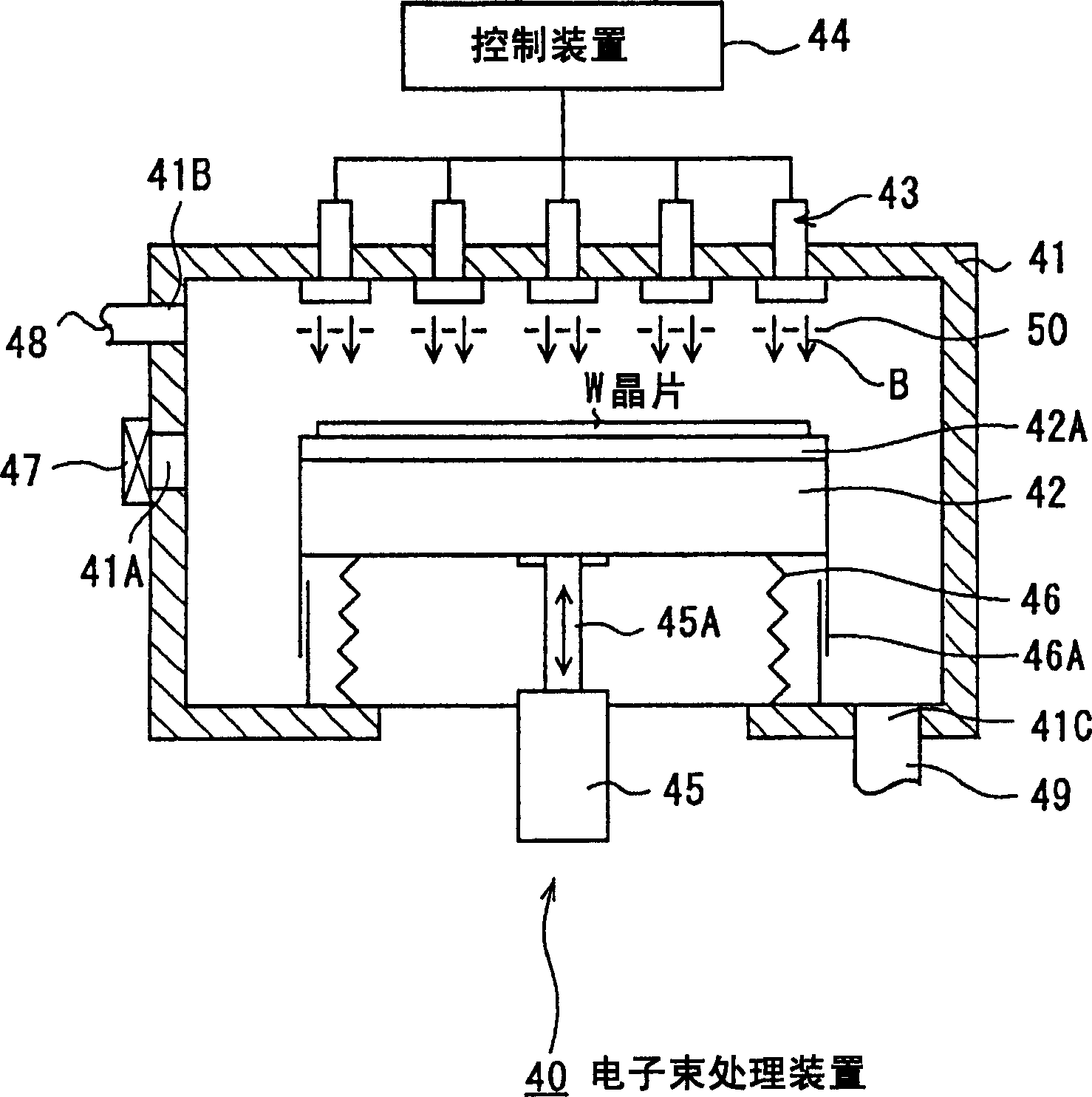
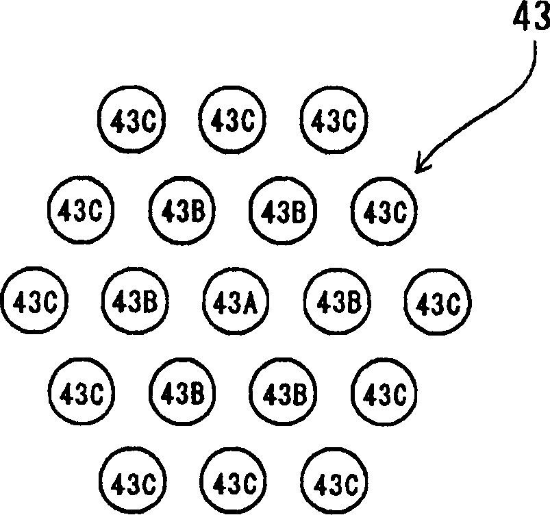
[0035] Below, according to Figure 1 to Figure 8 The illustrated embodiments illustrate the invention.

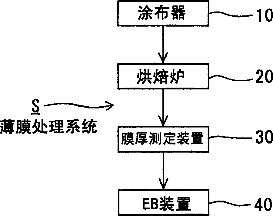
[0036] For example, if image 3 As shown, the thin film processing system S of the present embodiment includes: a spin coating device (spin coater) 10 for coating an SOD film material on the surface of an object to be processed (for example, a wafer); The downstream side of the device 10 and the baking furnace 20 that heat-treats the SOD film formed on the wafer; The film thickness measuring device 30 that is configured on the downstream side of the baking furnace 20 and measures the film thickness of the SOD film after heat treatment; On the downstream side of the thickness measuring device 30 , an electron beam processing device (EB device) 40 that irradiates an electron beam onto the SOD film based on the measurement result of the film thickness measuring device 30 . As the spin coater 10, the baking oven 20, and the film thickness measuring device 30 used at this time, ...


PUM


Abstract

To solve a problem that when a film such as a resist film or an interlayer insulating film is conventionally formed, it is difficult to make the film thickness uniform; for example, when an SOD film is formed using a spin coater, the film thickness is nonuniform as shown in Fig.(a), and remains as it is. The method to be disclosed of forming the film is, when the SOD film formed on a wafer W is irradiated with electron beams B from first, second, and third electron-beam tubes 43A, 43B, 43C, to control the respective outputs of the first, second, and third electron-beam tubes 43A, 43B, 43C in accordance with the film thickness distribution shown in Fig.6(a) to vary the dose quantity for each block as shown in Fig.6(b).

Description

technical field [0001] The present invention relates to a thin film processing method and a thin film processing system, in particular to a thin film processing method and a thin film processing system capable of performing thin film processing with a uniform film thickness, or removing charged charges on the film by a plasma processing device. Background technique [0002] With the high integration and high speed of semiconductor devices, the miniaturization of the wiring structure, the high precision of the wiring pattern of the resist film and the reduction of the capacitance between the wirings are becoming more and more important. That is, the higher the fineness of the wiring pattern, the more uniform the thickness of the resist film is required, and the uniform thickness of the interlayer insulating film is required for accurate etching. [0003] In the case of forming a resist film and an interlayer insulating film, for example, spin coating and a baking furnace are ...

Claims


Application Information

Patent Timeline
Patent Type & Authority Patents(China)
IPC IPC(8): H01L21/30H01L21/3105H01L21/205C23C16/56H01J37/317H01L21/00H01L21/02H01L21/263H01L21/312
CPCH01L21/312H01J37/317H01L21/67069H01L21/2636C23C16/56H01J2237/3156H01L21/67253H01J2237/004H01L21/02282H01L21/02274H01L21/02126H01L21/02351
Inventor 大西正滨学本多稔光冈一行岩下光秋
Owner TOKYO ELECTRON LTD
Features
  • R&D
  • Intellectual Property
  • Life Sciences
  • Materials
  • Tech Scout
  • Unparalleled Data Quality
  • Higher Quality Content
  • 60% Fewer Hallucinations
Learn More