Charged particle beam projection lithography with variable beam shaping

a technology of projection lithography and charge particle beam, applied in the field of projection reticles, can solve the problems of large integrated circuits, large size integrated circuits, and low throughput of probe-forming exposure tools, so as to achieve the effect of high precision and complexity, and large-scale integrated circuits

Inactive Publication Date: 2002-08-20
NIKON CORP
View PDF8 Cites 13 Cited by
  • Summary
  • Abstract
  • Description
  • Claims
  • Application Information

AI Technical Summary

Problems solved by technology

However, modern integrated circuit designs require feature sizes smaller than can be resolved using even very short wavelengths of light in the deep ultra-violet range even using sophisticated devices such as phase shift masks, off-axis illumination or optical proximity correction.
Therefore, the throughput of probe-forming exposure tools, even of the shaped-beam type, is too low to be economically feasible for high density, large scale integrated circuits even though exposures can be made at relatively high rate.
However, in the case of stencil reticles, complementary subfields are used to solve the "doughnut" problem of printing closed features; respective parts of which must be exposed from different patterns since annular patterns cannot be fabricated as a stencil.
The practical requirement of providing all necessary patterns on a reticle, however, presents a problem in that even a very minor change in the design or layout of the integrated circuit requires a new reticle to be made incorporating the change.
Reticles must be of extremely high precision and complexity as well as being defect-free and are thus extremely expensive to fabricate.
Thus, changes and improvements in existing integrated circuit designs may substantially increase the overall cost of manufacture over the economic lifetime of the design.
Local Coulomb effects are caused by the mutual repulsion of particles having the same charge and are manifested as both localized defocussing and therefore an increase in image blur where the exposure pattern is relatively more or less dense, and distortion of the pattern due to dislocation of the subfield features in regions where the density of the exposure pattern changes.
These blurs and distortions may or may not be tolerable in a particular design or portion thereof.
These problems are major obstacles to the successful practice of charged particle beam projection lithography since they present limitations on economic feasibility and fidelity of imaging and generally impose trade-offs therebetween.
Further, these problems are particularly intractable since they derive from unavoidable physical effects or force a trade-off between tool costs and tool throughput, which also forms a substantial economic cost component of the manufacturing process.

Method used


Image

  • Charged particle beam projection lithography with variable beam shaping
  • Charged particle beam projection lithography with variable beam shaping
  • Charged particle beam projection lithography with variable beam shaping

Examples


Embodiment Construction

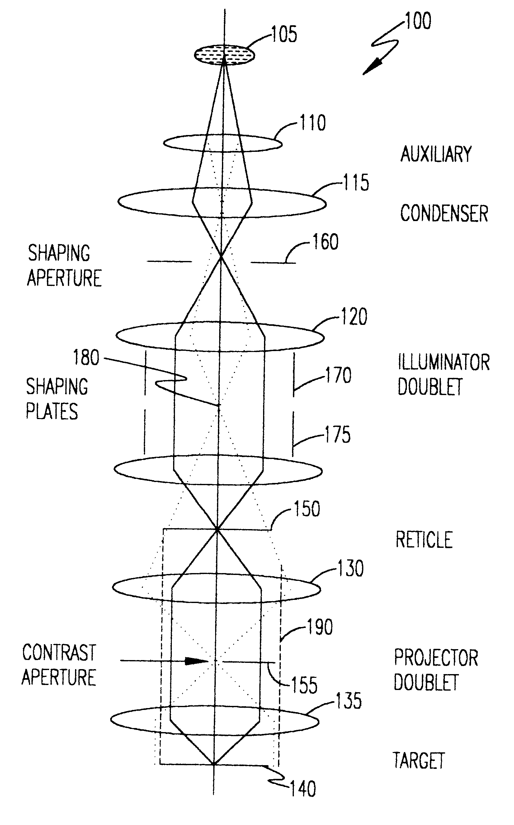
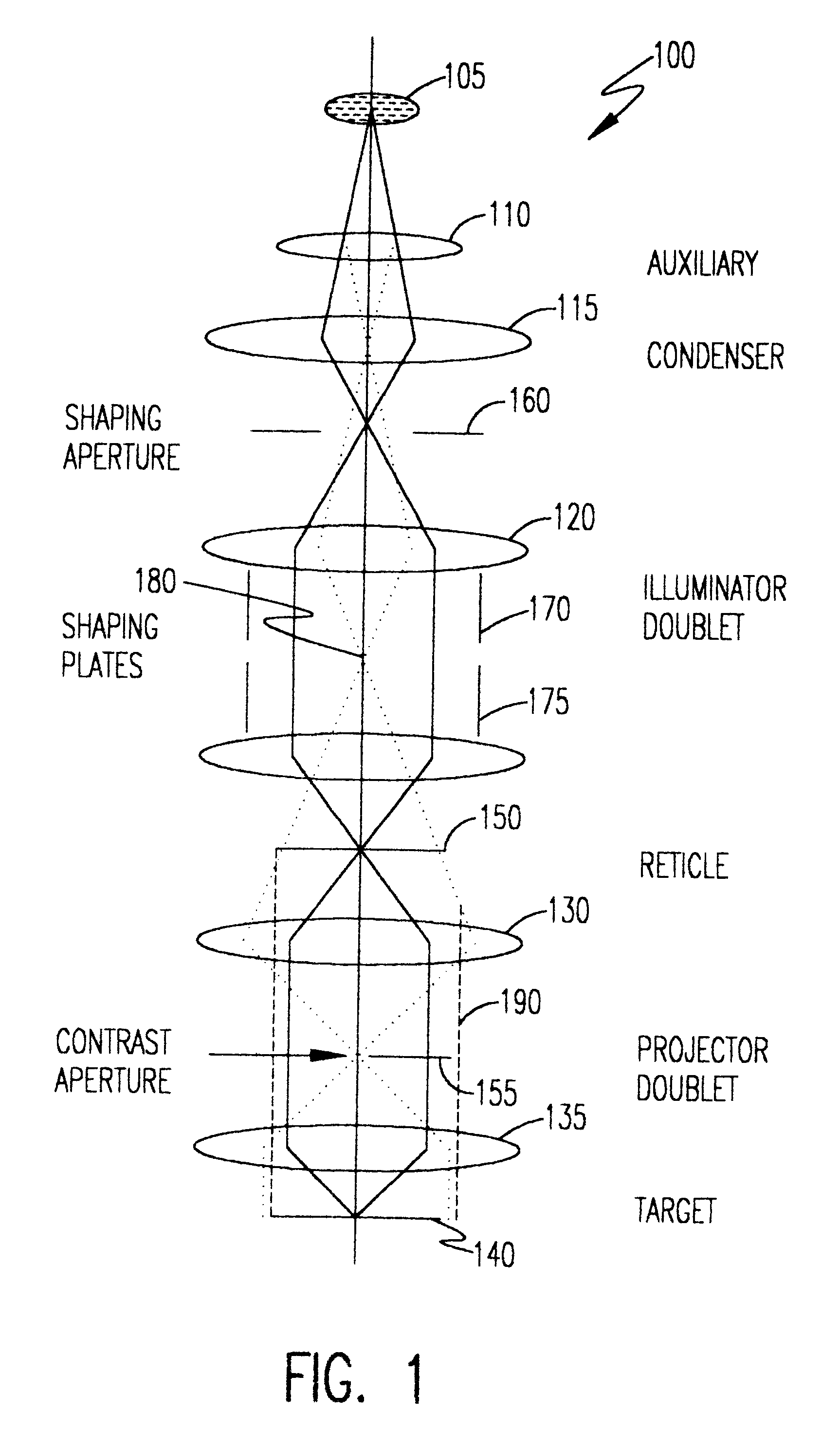
Referring now to the drawings, and more particularly to FIG. 1, there is shown, in highly schematic form, a charged particle beam column 100 in accordance with the invention. It should be understood that the preferred implementation of the invention employs an electron beam and, while the invention will be explained with reference thereto, the principles of the invention are also fully applicable to beams of ions, as well. Therefore, any reference to electrons and / or electron beams hereinafter should be understood as reflecting the preferred implementation and not as excluding other charged particles or charged particle beams to which the invention may also be applied.

The electron beam column 100 includes an electron (or other charged particle) source 105, a condenser lens arrangement 115, which may include one or more lenses and auxiliary lenses 110 used to position the source cross-over of the beam, an illuminator doublet 120, 125, to provide illumination of a reticle subfield, a ...


PUM

PropertyMeasurementUnit
sizeaaaaaaaaaa
sizeaaaaaaaaaa
areaaaaaaaaaaa

Abstract

Flexibility of a charged particle (e.g. electron) beam projection lithography tool is enhanced by filling a shaping aperture with the beam, projecting the image of the shaping aperture to a reticle subfield where the image preferably corresponds in size to a "clear" or "aperture" area in a subfield of the reticle and deflecting the beam across a selected portion thereof to develop a compound image which is projected onto the target (e.g. wafer). Deflection of the shaped beam onto the reticle aperture is preferably performed electrostatically with the center of deflection coincident with the source cross-over of the charged particle beam column to avoid motion of the beam at the contrast aperture which is used, possibly together with a beam tube, to collect particles scattered where the deflected beam overlaps the patterned areas of the reticle adjacent the reticle aperture. Fabrication of new reticles is thus avoided for minor design changes by provision of direct writing for the design changes while preserving a large portion of the benefits of high throughput of charged particle beam projection of reticle patterns to the target.

Description

1. Field of the InventionThe present invention generally relates to charged particle beam projection lithography exposure tools and, more particularly, to projection reticles used therein.2. Description of the Prior ArtLithographic processes are utilized in the manufacture of many diverse types of devices, particularly when very small areas must be selectively defined and / or operated upon, as in semiconductor integrated circuit manufacture. At least one lithographic process is invariably required for initial definition of locations and basic dimensions of devices such as transistors and capacitors in integrated circuits.Lithographic processes currently used for integrated circuit manufacture involve the selective exposure of areas of a resist coated on a surface. In general, depending on whether the resist is of a positive or negative type, subsequent development will selectively remove either the exposed or unexposed areas leaving other areas substantially unaffected. In the past, ...

Claims


Application Information

Patent Timeline
Patent Type & Authority Patents(United States)
IPC IPC(8): H01J37/317G03F1/16G03F7/20H01J37/147H01J37/305H01L21/027
CPCB82Y10/00B82Y40/00H01J37/3174
Inventor GORDON, MICHAEL S.
Owner NIKON CORP
Why Eureka
Try Eureka