Method for reducing leakage current on surface of base plate in thin film transistor

A technology for thin-film transistors and substrate surfaces, which is applied in the manufacture of circuits, electrical components, and semiconductor/solid-state devices. Reduce stray capacitance and improve electrical performance

Inactive Publication Date: 2006-09-13
AU OPTRONICS CORP
View PDF0 Cites 0 Cited by
  • Summary
  • Abstract
  • Description
  • Claims
  • Application Information

AI Technical Summary

Problems solved by technology

Due to the high dielectric constant of silicon nitride, the stray capacitance derived from it is also relatively high, which can easily cause abnormal images
[0006] Moreover, the silicon nitride process has its weak thickness limitation, generally speaking, its thickness is controlled to be less than 5000 angstroms, so the resistance to the invasion of water vapor and other impurities is poor, and it is easy to cause the increase of surface leakage current and affect the components normal operation of

Method used


Image

  • Method for reducing leakage current on surface of base plate in thin film  transistor
  • Method for reducing leakage current on surface of base plate in thin film  transistor
  • Method for reducing leakage current on surface of base plate in thin film  transistor

Examples


Embodiment Construction

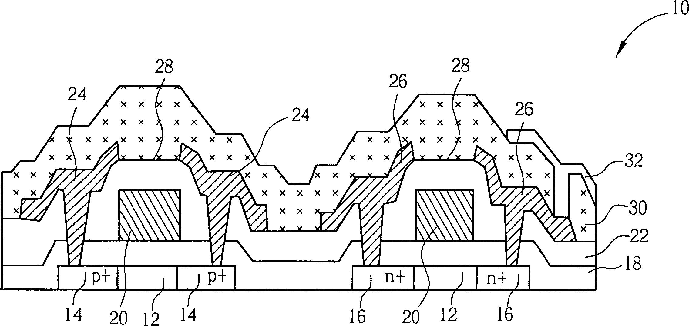
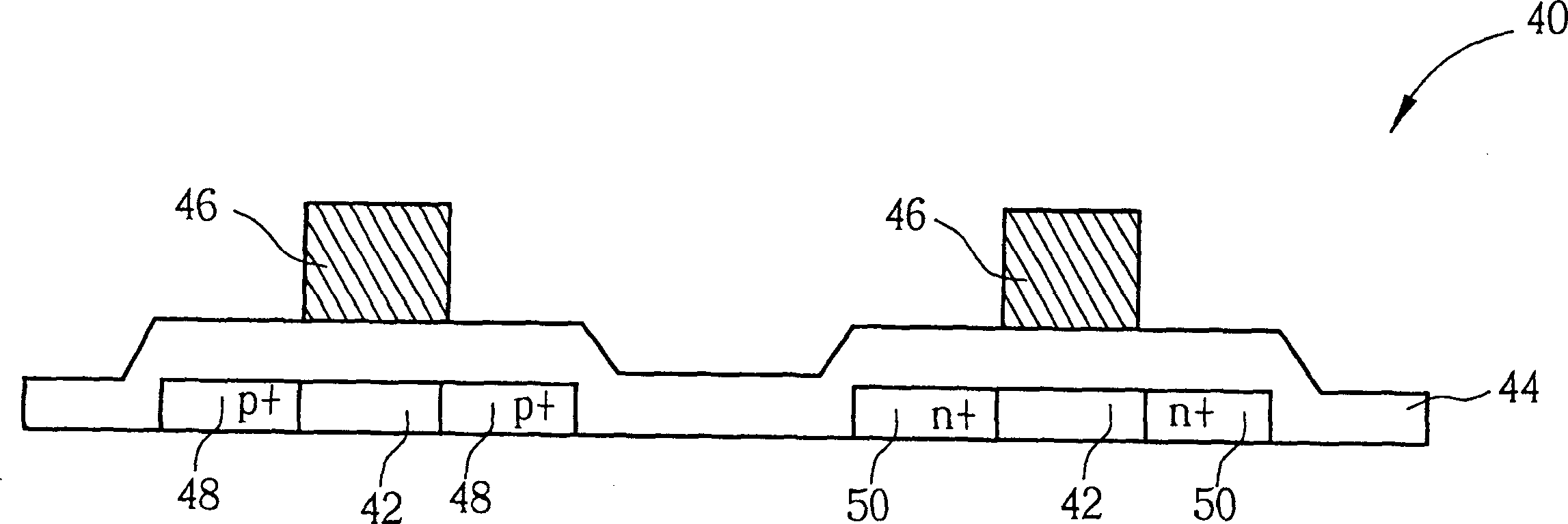
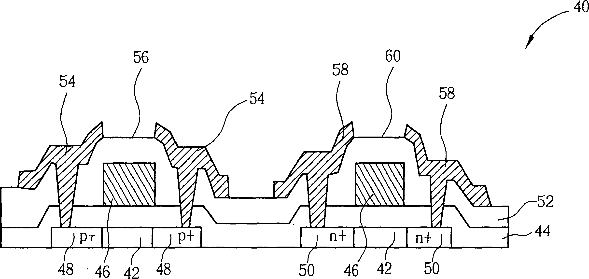
[0023] Please refer to Figure 2 to Figure 5 , Figure 2 to Figure 5 It is a schematic diagram of the method for manufacturing a thin film transistor substrate of the present invention. Such as figure 2 As shown, a semiconductor layer 42 is first formed on the surface of a thin film transistor substrate 40, and then a plurality of doped regions 48 and 50 are formed in the semiconductor layer 42 by using different types of dopants as the source / drain of the thin film transistor. , and define the element type as N-type TFT or P-type TFT. Next, a gate insulating layer 44 and a first metal layer 46 are sequentially formed on the surface of the semiconductor layer 42, and part of the first metal layer 46 is removed by photolithography and etching processes to form a plurality of gates on the semiconductor layer 42. Pole 46. In addition, in other embodiments of the present invention, the gate 46 can also be used as an ion implantation mask after the gate 46 is formed, so as to ...


PUM

PropertyMeasurementUnit
thicknessaaaaaaaaaa

Abstract

First, multiple Thin Film Transistors (TFT) are formed on a base plate. Next, an insulation layer and a metal layer are formed on TFT in sequence. The metal layer includes a source pole and a drain pole connected to each TFT, and there is a channel region between the source pole and the drain pole. Then, an organic material layer is covered on the metal layer and the insulation layer, and a transparent conducting layer is formed on the organic material layer. In the procedure of forming the organic material layer, since the insulation layer is densified synchronistically, route of current leakage of the base plate is blocked out so as to reduce current leakage on surface.

Description

technical field [0001] The invention relates to a method for reducing the surface leakage current of a thin film transistor substrate, in particular to a method for reducing the surface leakage current of a thin film transistor substrate of a liquid crystal display. Background technique [0002] The liquid crystal display panel structure consists of a thin-film transistor substrate (TFT substrate), a color filter substrate (CF substrate), and a liquid crystal layer disposed between the thin-film transistor substrate and the filter substrate. constituted. The thin film transistor substrate includes a matrix of pixels composed of multiple rows of data lines and multiple columns of scanning lines, and a plurality of pixel driving circuits composed of electronic components such as thin film transistors and capacitors are respectively arranged on each data line and each scanning line of the intersection. For each pixel, the image data signal transmitted by the data line will be...

Claims


Application Information

Patent Timeline
Patent Type & Authority Patents(China)
IPC IPC(8): H01L21/336H01L21/00G02F1/133
Inventor 胡晋玮陈坤宏
Owner AU OPTRONICS CORP
Why Eureka
Try Eureka