Check patentability & draft patents in minutes with Patsnap Eureka AI!

Structure of mask ROM and method for manufacturing the same

A technology of read-only memory and manufacturing method, which is applied in semiconductor/solid-state device manufacturing, electric solid-state devices, semiconductor devices, etc., and can solve data errors in read-only memory storage units, poor product reliability, and affect storage unit operating characteristics, etc. problems, to achieve the effect of reducing production costs and reducing delivery time

Inactive Publication Date: 2006-11-22
MACRONIX INT CO LTD
View PDF0 Cites 0 Cited by
  • Summary
  • Abstract
  • Description
  • Claims
  • Application Information

AI Technical Summary

Problems solved by technology

Such ROMs take longer to order and require a dedicated code mask for the channel ion implantation step
Moreover, when the channel ion implantation step is performed, if the position of the ion implantation block is misaligned, it will directly affect the operating characteristics of the storage unit, causing data errors in the ROM storage unit, resulting in product failures. worsening reliability

Method used


Image

  • Structure of mask ROM and method for manufacturing the same
  • Structure of mask ROM and method for manufacturing the same
  • Structure of mask ROM and method for manufacturing the same

Examples


Embodiment Construction

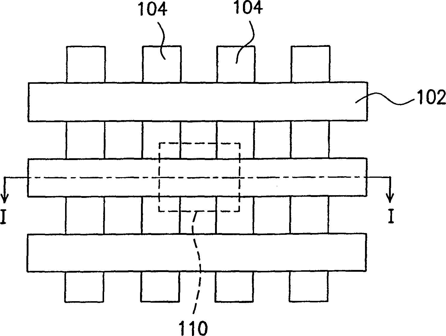
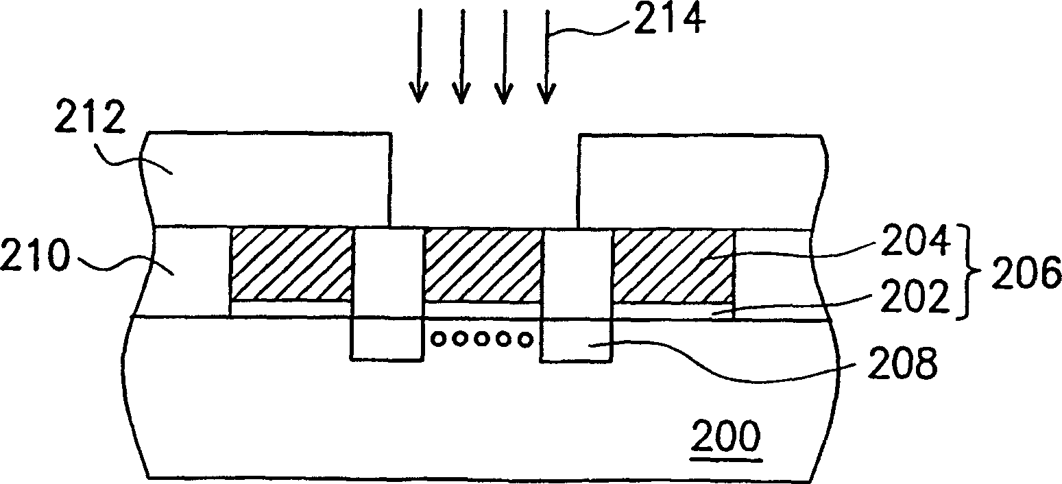
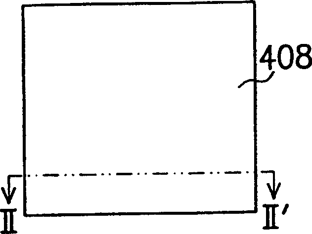
[0047] The invention provides a structure of a mask-mode read-only memory and a manufacturing method thereof. Figure 3A to Figure 3G It is a top view of a memory cell region of a mask-mode ROM according to an embodiment of the present invention. Figure 4A to Figure 4G It is a sectional view of a manufacturing process of a mask-mode ROM according to an embodiment of the present invention. exist Figure 4A and Figure 4G The middle substrate 400 can be divided into a memory cell area 402 and a peripheral circuit area 404, wherein the memory cell area 402 shown in each figure is respectively Figure 3A to Figure 3G The cross-sectional view of the structure along the line II-II'.

[0048] First, please refer to Figure 3A and Figure 4A , providing a substrate 400, such as a semiconductor silicon substrate. The substrate 400 can be divided into a memory cell area 402 and a peripheral circuit area 404 .

[0049] Next, a plurality of isolation structures 406 are formed in t...


PUM


Abstract

A method for manufacturing a mask-type read-only memory, the method sequentially forms a silicon monoxide / silicon nitride / silicon oxide composite layer and a plurality of gates on a substrate, and the silicon oxide between any gate and the substrate / silicon nitride / silicon oxide composite layer as a predetermined coding area. Then, a plurality of bit lines are formed in the substrate between the gates, and a plurality of word lines electrically connected with the gates are formed on the substrate. Then, a chemical vapor deposition anti-reflection material layer and an inner dielectric layer are formed on the substrate. Then, an encoding process is carried out, using the chemical vapor deposition anti-reflection layer as the encoding mask, and irradiating the substrate with ultraviolet light, so that the predetermined encoding area under the gate exposed by the encoding window forms a plurality of writing encoding areas, and then writes in the encoding window A plug is formed inside.

Description

technical field [0001] The present invention relates to a structure and a manufacturing method of a read-only memory (ROM), and in particular to a structure and a manufacturing method of a mask-mode read-only memory (Mask ROM). Background technique [0002] Since the read-only memory has the non-volatile characteristic that the data stored therein will not be lost due to power interruption, many electrical products must have this type of memory in order to maintain the normal operation of the electrical product when it is turned on. The most basic type of read-only memory is the mask-mode read-only memory. Generally, the commonly used mask-mode read-only memory uses channel transistors as storage units, and selectively implants ions into designated channels during the programming (Program) stage. area, by changing the threshold voltage (Threshold Voltage) to achieve the purpose of controlling the memory cell to be turned on (On) or turned off (Off) during the read operation....

Claims


Application Information

Patent Timeline
Patent Type & Authority Patents(China)
IPC IPC(8): H01L21/8246H01L27/112H10B20/00
Inventor 郭东政刘建宏潘锡树黄守伟
Owner MACRONIX INT CO LTD
Features
  • R&D
  • Intellectual Property
  • Life Sciences
  • Materials
  • Tech Scout
  • Unparalleled Data Quality
  • Higher Quality Content
  • 60% Fewer Hallucinations
Learn More