Ball grid array semiconductor package

A ball grid array, semiconductor technology, applied in the direction of semiconductor devices, semiconductor/solid-state device components, electric solid-state devices, etc., can solve the problems of destruction, inability to change, insufficient change, etc.

Inactive Publication Date: 2006-11-29
SILICONWARE PRECISION IND CO LTD
View PDF2 Cites 0 Cited by
  • Summary
  • Abstract
  • Description
  • Claims
  • Application Information

AI Technical Summary

Problems solved by technology

[0006] However, the above-mentioned method of using laser technology still has many disadvantages; one is that the method must prepare a laser generator to generate corresponding laser light to complete, and the manufacturing cost of this laser generator is high, so it will greatly increase the production of packaged products cost
In addition, cutting conductive traces with a laser will cause pollution, and additional cleaning procedures are required for the package, which further increases the cost; and the energy of the laser needs to be controlled accurately, because the internal structure of the semiconductor package is very fine. A slight error in the laser energy for cutting the conductive traces will cause damage to other parts of the semiconductor package (such as the lower conductive traces) and affect the yield of finished products
In view of this, the way to solve the above problems is to let no other conductive traces be laid under the conductive traces for burning and cutting, or to pre-lay a copper layer under the conductive traces for burning and cutting, so that the energy of the laser will not damage other conductive traces; however, this practice places significant constraints on circuit layout on the substrate, especially for products with high-density routing
In addition, the conductive traces after burning and cutting cannot be restored to the original electrical conduction state, that is, once the packaged product has been burnt and cut to form certain specific functions, the product cannot be changed to have other functions, so The changes that can be provided in response to market demand are still insufficient

Method used


Image

  • Ball grid array semiconductor package
  • Ball grid array semiconductor package
  • Ball grid array semiconductor package

Examples


Embodiment 1

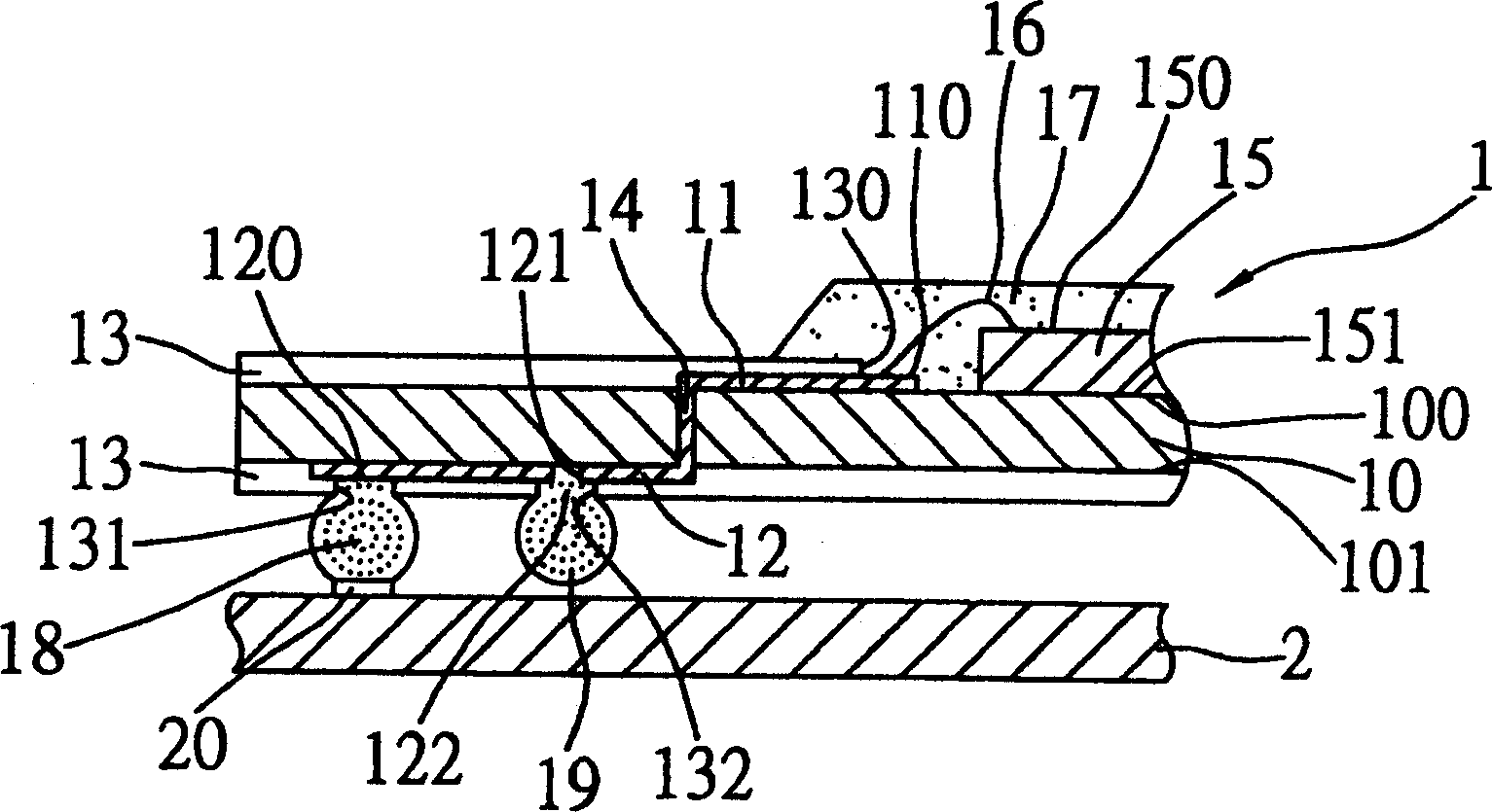
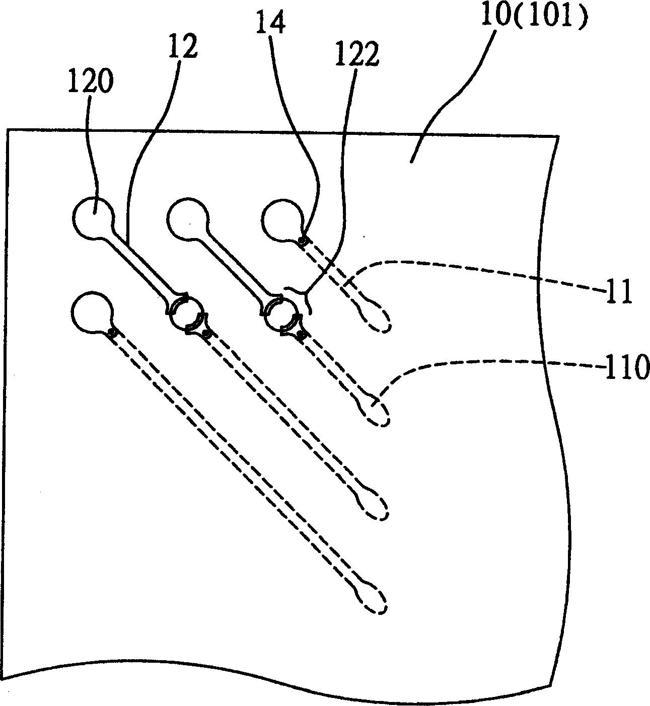
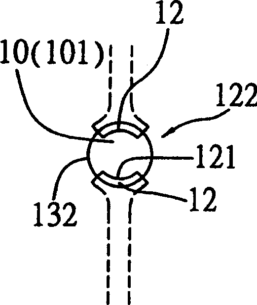
[0026] Such as figure 1As shown, the semiconductor package 1 of Embodiment 1 of the present invention is a ball grid array packaging structure using a substrate 10 as a chip carrier (Chip Carrier), and the substrate 10 can be made of existing resin materials, such as epoxy resin (Epoxy Resin) ), polyimide (Polyimide) resin, BT (Bismaleimide Triazine) resin, FR4 resin, FR5 resin, etc. The substrate 10 has an upper surface 100 and an opposite lower surface 101, a plurality of first conductive traces 11 are laid on the upper surface 100 of the substrate 10, and a plurality of second conductive traces are formed on the lower surface 101 of the substrate 10 The wire 12 , the conductive traces 11 , 12 each have a terminal 110 , 120 . The conductive traces 11, 12 are formed by passing at least one copper foil (Copper Foil, not shown) bonded on the upper and lower surfaces 100, 101 of the substrate 10 through existing exposure (Exposing), developing (Developing) , etching (Etching) ...

Embodiment 2

[0037] Figure 6 A semiconductor package 1' of Embodiment 2 of the present invention is shown. As shown in the figure, the structure of this semiconductor package 1' is roughly the same as that of Embodiment 1 ( figure 1 ) is the same as the semiconductor package 1 , the difference is that the discontinuous pads 122 and the first solder balls 19 are arranged on the upper surface 100 of the substrate 10 . That is, the discontinuous pad 122 is formed on the upper surface 100 of the substrate 10 at the non-terminal (or welding finger) 110 position of the predetermined first conductive trace 11, so that the discontinuous pad 122 and the first implanted thereon The solder ball 19 is not covered by the encapsulant 17, so that the first solder ball 19 can be removed or pushed away from the discontinuous pad 122 as required; also, the discontinuous pad 122 and the first solder ball 19 are arranged on the The upper surface 100 of the substrate 10 does not occupy the area for the inpu...

Embodiment 3

[0039] Figure 7A Shows the semiconductor package 1 " of embodiment 3 of the present invention. As shown in the figure, the structure of this semiconductor package 1 " is roughly the same as that of embodiment 1 ( figure 1 ) is the same as the semiconductor package 1, the difference is that the terminal portion of the predetermined second conductive trace 12 on the lower surface 101 of the substrate 10 is to form a discontinuous pad 122 instead of forming an input / output pad; that is, the The second conductive trace 12 formed with the discontinuous pad 122 is electrically connected to the solder finger 110 connected to the solder wire 16 on the upper surface 100 of the substrate 10 through the corresponding conductive through hole 14, and is not connected to the solder finger 110 as an input / output The second solder ball 18 or the output / input pad 120 at the end forms an electrical connection.

[0040] When the functions of these chips are to be controlled, it can be realized...


PUM


Abstract

The ball grid array semiconductor package is manufactured through forming discontinuous fractures in the set parts of conducting trace on the substrate to expose the soldering inhibitor in the fractures and adjacent trace parts and to form discontinuous soldering pads; and selectively implanting soldering balls onto the discontinuous soldering pads to make the conducting trace with soldering balls form conducting path. The soldering balls are jointed to the soldering pads in unstable state and may be removed easily to make the conducting trace broken; and the removed soldering balls may be re-implanted to the soldering pads to restore the electric conductivity of the conducting trace.

Description

technical field [0001] The present invention relates to a semiconductor package, in particular to a ball grid array (BallGrid Array, BGA) semiconductor package, using a plurality of solder balls (Solder Ball) as input / output (Input / Output, I / O) The terminal enables the chip in the semiconductor package to be electrically connected to the outside world. Background technique [0002] The semiconductor package is characterized in that at least one semiconductor chip is loaded on a chip carrier (such as a substrate, a lead frame, etc.), and the chip is connected by a bonding wire (Bonding Wire) or a solder bump (that is, a flip-chip structure, Flip Chip) and other conductive components are electrically connected to the chip carrier, and then resin materials such as epoxy resin (Epoxy Resin) are used to form an encapsulant that covers the chip and conductive components, so that the chip is airtightly isolated from the outside world ; The packaged chip can be integrated with an e...

Claims


Application Information

Patent Timeline
Patent Type & Authority Patents(China)
IPC IPC(8): H01L23/48H01L23/28H01L23/52H01L23/12
CPCH01L2924/15192H01L2224/48227H01L2224/48091H01L2924/15311H01L2224/49175H01L2224/05554H01L2924/181H01L2924/00014H01L2924/00H01L2924/00012
Inventor 普翰屏黄建屏
Owner SILICONWARE PRECISION IND CO LTD
Why Eureka
Try Eureka