

Material with composite substrate of (Mg, Cd) In2O4/MgAl/204 and its prepn method
A composite substrate, mgal2o4 technology, applied in semiconductor/solid-state device manufacturing, semiconductor lasers, lasers, etc., can solve the problems of increasing device volume, less use, lattice mismatch, etc., and achieve simple preparation process, easy operation, Effect of small lattice mismatch
- Summary
- Abstract
- Description
- Claims
- Application Information
AI Technical Summary
Problems solved by technology
Method used
Image

Examples
Embodiment 1
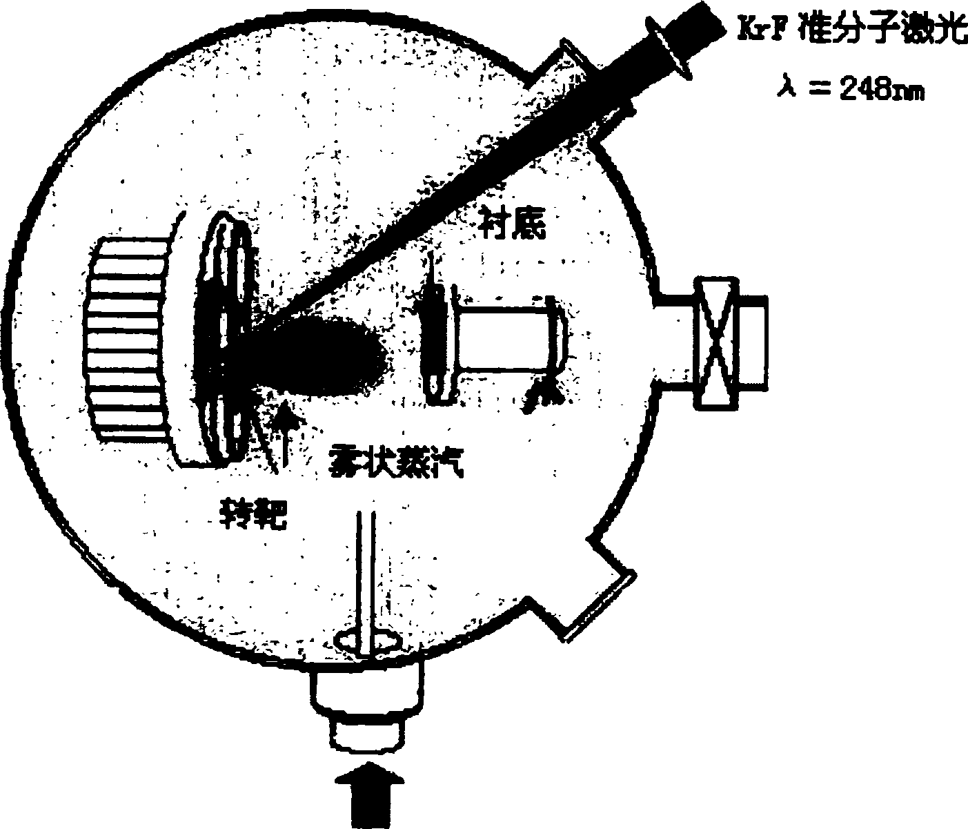
[0030] The polished and cleaned MgAlO 4 The single crystal substrate is sent to the pulsed laser deposition PLD system to prepare (Mg, Cd) In 2 o 4 thin film, (Mg,Cd)In 2 o 4 The source uses more than 99.999% (Mg, Cd) In 2 o 4 Polycrystalline target. The system uses a KrF excimer laser with a pulse width of 25-30ns, and the lasing wavelength is 248nm. 2 The energy density of the concentrated light is irradiated to the (Mg, Cd)In in the vacuum device through the optical window 2 o 4 target, depositing (Mg, Cd)In in an oxygen-rich atmosphere 2 o 4 thin film, MgAl 2 o 4 The single crystal substrate temperature is 200°C, and the (Mg, Cd)In 2 o 4 The thickness of the film was 300 nm. Then the (Mg, Cd)In obtained in the previous step 2 o 4 / MgAl 2 o 4 The sample is placed in an annealing furnace, and the temperature is raised to 10,000°C for annealing treatment to obtain (Mg, Cd)In 2 o 4 single crystal capping layer, resulting in (Mg, Cd)In 2 o 4 / MgAl 2 o 4 ...
Embodiment 2
[0032] The polished and cleaned MgAl 2 o 4 The single crystal substrate is sent to the pulsed laser deposition PLD system to prepare (Mg, Cd) In 2 o 4 thin film, (Mg,Cd)In 2 o 4 The source uses more than 99.999% (Mg, Cd) In 2 o 4 Polycrystalline target. The system uses a KrF excimer laser with a pulse width of 25-30ns (nanoseconds), and the lasing wavelength is 248nm. 2 The energy density of the concentrated light is irradiated to the (Mg, Cd)In in the vacuum device through the optical window 2 o 4 target, depositing (Mg, Cd)In in an oxygen-rich atmosphere 2 o 4 thin film, MgAl 2 o 4 The single crystal substrate temperature is 100°C, and the (Mg, Cd)In 2 o 4 The thickness of the film was 100 nm. Then the (Mg, Cd)In obtained in the previous step 2 o 4 / MgAl 2 o 4 The sample is placed in an annealing furnace, and the temperature is raised to 700°C for annealing treatment to obtain (Mg, Cd)In 2 o 4 single crystal capping layer, resulting in (Mg, Cd)In 2 o 4...
Embodiment 3
[0034] The polished and cleaned MgAl 2 o 4 The single crystal substrate is sent to the pulsed laser deposition PLD system to prepare (Mg, Cd) In 2 o 4 thin film, (Mg,Cd)In 2 o 4 The source uses more than 99.999% (Mg, Cd) In 2 o 4 Polycrystalline target. The system uses a KrF excimer laser with a pulse width of 25-30ns, and the lasing wavelength is 248nm. 2 The energy density of the concentrated light is irradiated to the (Mg, Cd)In in the vacuum device through the optical window 2 o 4 target, depositing (Mg, Cd)In in an oxygen-rich atmosphere 2 o 4 thin film, MgAl 2 o 4 The single crystal substrate temperature is 300°C, and the (Mg, Cd)In 2 o 4 The thickness of the film was 500 nm. Then the (Mg, Cd)In obtained in the previous step 2 o 4 / MgAl 2 o 4 The sample is placed in an annealing furnace, and the temperature is raised to 1500°C for annealing treatment to obtain (Mg, Cd)In 2 o 4 single crystal capping layer, resulting in (Mg, Cd)In 2 o 4 / MgAl 2 o ...
PUM
| Property | Measurement | Unit |
|---|---|---|
| lattice constant | aaaaa | aaaaa |
| melting point | aaaaa | aaaaa |
Abstract
Description
Claims
Application Information