Polycrystalline silicon thin film and method for preparing polycrystalline silicon thin film by amorphous silicon low-temperature induction

A polysilicon thin film, low temperature induced technology, used in semiconductor devices, final product manufacturing, sustainable manufacturing/processing, etc., can solve the problems of slow crystallization rate of metal induction method, achieve increased crystallization rate, low nucleation barrier, contact The effect of increasing the area

Inactive Publication Date: 2011-09-28
HANGZHOU AMPLESUN SOLAR TECH
View PDF0 Cites 1 Cited by
  • Summary
  • Abstract
  • Description
  • Claims
  • Application Information

AI Technical Summary

Problems solved by technology

[0004] The technical problem to be solved and the technical task proposed by the present invention are to overcome the defects of the slow crystallization rate of the existing metal induction method, and provide a polysilicon film and a method for preparing a polysilicon film by low-temperature induction of amorphous silicon

Method used


Image

  • Polycrystalline silicon thin film and method for preparing polycrystalline silicon thin film by amorphous silicon low-temperature induction
  • Polycrystalline silicon thin film and method for preparing polycrystalline silicon thin film by amorphous silicon low-temperature induction

Examples


Embodiment 1

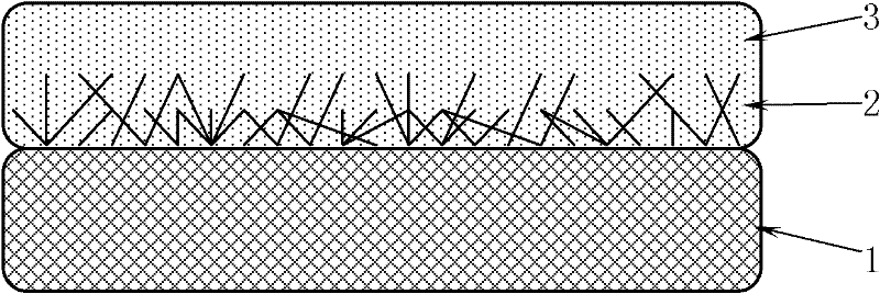
[0015] 1) Tin oxide transparent conductive glass (F-SNO 2 ) is the substrate 1, and a titanium silicide thin film layer and a titanium silicide nanowire composite structure are deposited on the substrate 1 by chemical vapor deposition. The titanium silicide nanowires include nanowires, nanonails, nanorods, and nanowire clusters, in the form of TiSi crystal Mutually;

[0016] 2) Depositing a 1 μm amorphous silicon film layer on the titanium silicide film and titanium silicide nanowire composite structure prepared in step 1) by plasma chemical vapor deposition at 13.56 MHz;

[0017] 3) Annealing and heat-treating the amorphous silicon thin film layer prepared in step 2) at 400° C. for 1 h, so that the titanium silicide nanowire induces the crystallization of the amorphous silicon thin film layer into a polycrystalline silicon thin film layer with large crystal grains, and finally obtains figure 1 Large grain polysilicon thin film shown.

Embodiment 2

[0019] 1) Using zinc oxide transparent conductive glass (Ag-ZnO) as the substrate, a layer of titanium silicide film and titanium silicide nanowire composite structure is deposited on the substrate 1 by chemical vapor deposition method. Titanium silicide nanowires include nanowires, nanonails, Rocket-shaped nanowires in the TiSi crystal phase;

[0020] 2) Depositing a layer of 2 μm amorphous silicon film layer on the titanium silicide film and titanium silicide nanowire composite structure prepared in step 1) by plasma chemical vapor deposition at 13.56MHZ;

[0021] 3) Annealing and heat-treating the amorphous silicon thin film layer prepared in step 2) at 400°C for 2 hours, so that the titanium silicide nanowires induce the crystallization of the amorphous silicon thin film layer into a polycrystalline silicon thin film layer with large grains, and finally obtain figure 1 Large grain polysilicon thin film shown.

Embodiment 3

[0023] 1) Tin oxide transparent conductive glass (F-SNO 2 ) is the substrate, and the titanium silicide nanowires are prepared on the substrate 1 by the solid-state reaction method. 2 crystal phase;

[0024] 2) Depositing a 3 μm amorphous silicon film layer on the titanium silicide nanowire prepared in step 1) by magnetron sputtering;

[0025] 3) The amorphous silicon thin film prepared in step 2) is annealed and heat-treated at 400°C for 2 hours, so that the titanium silicide nanowire induces the crystallization of the amorphous silicon thin film layer into a polycrystalline silicon thin film layer with large grains, and finally obtains figure 1 Large grain polysilicon thin film shown.


PUM


Abstract

The invention discloses a method for preparing a polycrystalline silicon thin film by amorphous silicon low-temperature induction, belonging to the technical field of thin-film solar battery. The method overcomes the disadvantage of slow crystallization rate of the existing metal induction method. According to the invention, a titanium silicide nano-wire layer and an amorphous silicon thin film layer are sequentially deposited on a substrate from bottom to top, wherein the titanium silicide nano-wire layer induces the amorphous silicon thin film layer to form a polycrystalline silicon thin film layer, thereby forming a polycrystalline silicon thin film having a three-layer composite structure consisting of the substrate, a transition layer with coexisting titanium silicide nano-wire and polycrystalline silicon thin film, and the polycrystalline silicon thin film layer. On one hand, the crystallization of the amorphous silicon thin film can be induced at a lower crystallization temperature easily since the titanium silicide nano-wire is used as an inducer; on the other hand, the titanium silicide nano-wire with a huge specific surface area can increase the contact area between the induction layer and the amorphous silicon, thereby increasing the nucleation number in the initial crystallization stage of the amorphous silicon and greatly improving the crystallization rate; and the entire crystallization process is completed in 2 to 4 hours.

Description

technical field [0001] The invention belongs to the technical field of thin-film solar cells, in particular to a polycrystalline silicon thin film and a method for preparing the polycrystalline silicon thin film by low-temperature induction of amorphous silicon. Background technique [0002] Photovoltaic power generation, as an important new renewable green energy, has been widely researched and utilized by countries all over the world; among many solar cells, silicon-based solar cells have the advantages of abundant raw materials and non-toxicity, and have become the main body of the solar cell market today, especially Polycrystalline silicon cells have high efficiency, relatively simple and reasonable production process and production cost. Judging from the research and development trend of the battery market, which prioritizes battery efficiency and production cost, polysilicon batteries are bound to become thinner. At present, there are a lot of researches on the prepar...

Claims


Application Information

Patent Timeline
Patent Type & Authority Applications(China)
IPC IPC(8): H01L31/0352H01L31/18
CPCY02P70/50
Inventor 李媛吴兴坤郝芳周丽萍杨晗琼
Owner HANGZHOU AMPLESUN SOLAR TECH
Why Eureka
Try Eureka