Method of preparing boron-phosphor-silicon fluorine glass

A technology of borophosphosilicate glass and fluoroalkoxysilane, which is applied in the field of making fluorine-doped borophosphosilicate glass, and can solve problems such as the viscosity reduction of dielectric films

Inactive Publication Date: 2007-02-21
IBM CORP +2
View PDF4 Cites 0 Cited by
  • Summary
  • Abstract
  • Description
  • Claims
  • Application Information

AI Technical Summary

Problems solved by technology

This breaks the oxygen bridge bonds between silicon a...

Method used


Image

  • Method of preparing boron-phosphor-silicon fluorine glass
  • Method of preparing boron-phosphor-silicon fluorine glass
  • Method of preparing boron-phosphor-silicon fluorine glass

Examples


Embodiment Construction

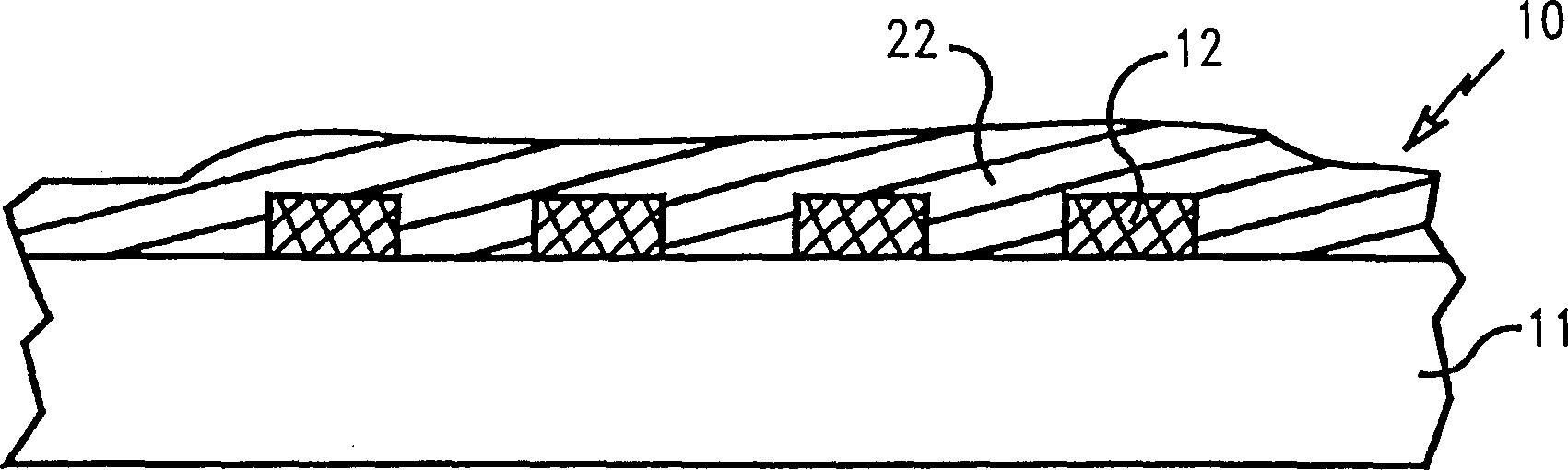
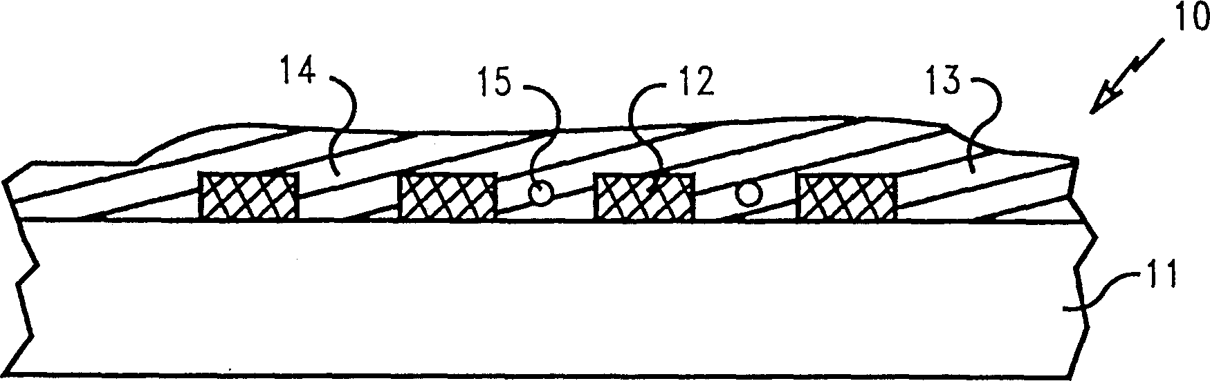
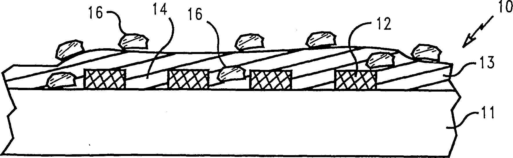
[0030] In describing the preferred embodiment of the invention, reference will be made to Figure 1-4 , wherein the same reference numerals represent the same elements of the present invention. The various elements of the invention in the figures are not necessarily drawn to scale.

[0031] According to the present invention, a fluorine-containing BPSG insulating planar layer (hereinafter referred to as F-BPSG) is formed on the surface of semiconductor wafers and other electronic component substrates. This F-BPSG layer is characterized as being substantially free of voids and surface crystals, and is a glass layer that can be easily reflowed at relatively low reflow temperatures consistent with presently proposed semiconductor wafer fabrication processes.

[0032] The term "semiconductor wafer" as used herein is meant to include wafer surface structures such as bumped leads, trenches, and transistors. The composition of structures on the surface of a semiconductor wafer is c...


PUM


Abstract

An equipment and method for producing fluorine-doped B-P-Si glass (F-BPSG) on a device through low-pressure CVD process. On a substrate with gap as narrow as 0.10 micron and structure of shape ratio of 6 to 1, F-BPSG is a layer with basically to void and no grain. The reactant gases include sources comprising B and P dopant, oxygen and the mixture of TEOS and FTES. F-BPSG is deposited at 750-850 deg.c temperature and under 1-3 torr pressure, and is annealed preferably in similar conditions to level the surface. Both F-BPSG and semiconductor chip with F-BPSG layer are provided.

Description

technical field [0001] The present invention relates to semiconductor electronic components and methods of manufacture thereof, and more particularly to improved borophosphosilicate glass for use as substantially void-free layers on semiconductor wafers as narrow as 0.10 μm and with aspect ratios as high as 6:1 , and methods including making the glass layers at reflow temperatures of about 800° C. lower than currently suggested manufacturing requirements. Background technique [0002] In the manufacture of semiconductor electronic components, the components must be encapsulated in glass, or glass is used as an interlayer dielectric film. Typically, the glass layer is SiO deposited on the wafer surface by chemical vapor deposition (CVD) 2 layer. The need for finer circuit patterns and higher circuit densities due to growing demands from the industry has necessitated the development of improved glass layers to layer semiconductor surfaces in the manufacturing process. Of pa...

Claims


Application Information

Patent Timeline
IPC IPC(8): H01L21/316C03B19/14
Inventor 马库斯·基尔绍夫阿什马·查克拉瓦蒂马西斯·伊尔格凯文·A·迈克金利桑·V·恩古恩迈克尔·J·沙皮罗
Owner IBM CORP
Why Eureka
Try Eureka