Nanometer structure forming method and special equipment therefor
A nanostructure and special equipment technology, applied in the field of metal surface treatment, can solve problems such as unqualified and difficult to obtain nanostructures
- Summary
- Abstract
- Description
- Claims
- Application Information
AI Technical Summary
Problems solved by technology
Method used
Image
Examples
Embodiment 1
[0034] Surface treatment on metal parts to obtain a layer of nanostructures, the specific steps are:
[0035] 1) Apply mechanical stress and / or thermal stress to the metal part to be treated; the stress value is less than the yield stress of the metal part material;
[0036] 2) For a defined duration, with a defined velocity, a defined distance, the same impact point, a variable angle of incidence and a limited number of fully spherical projectiles that can be repeatedly used over a long period of time on the entire surface of the metal part to be treated. a spray treatment;
[0037] 3) With the movement of the impact point, step 2) is repeatedly carried out so that the impact point covers all the surfaces to be treated of the metal part;
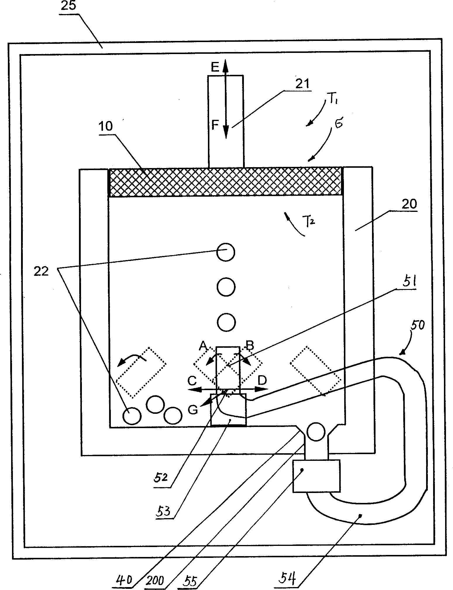
[0038] Its special equipment: such as figure 1 As shown, in a soundproof cavity 25, including projectiles 22, said projectiles 22 are completely spherical, with a certain size, speed and quantity; also include a container 20, a fixed part...
Embodiment 2
[0055] The difference from Example 1 is:
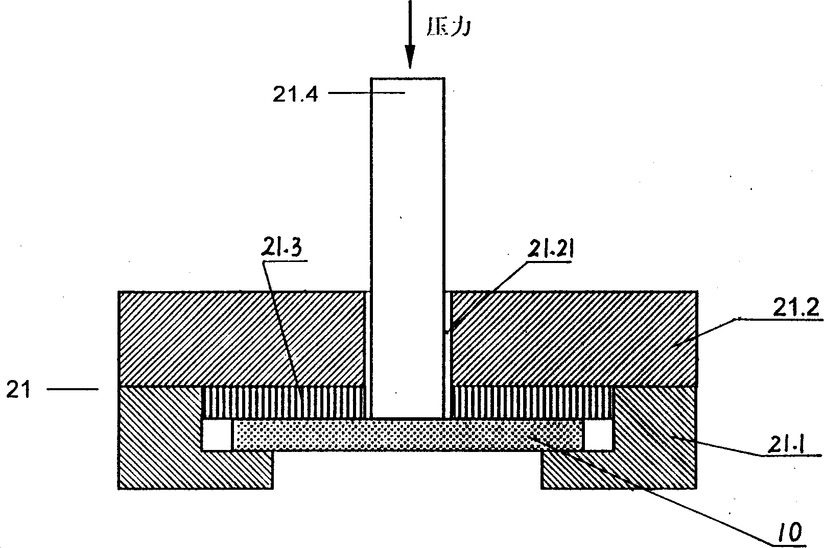
[0056] When it is desired to obtain a nanostructured surface layer with a thickness of tens to hundreds of microns, the surface treatment of the metal part 10 to be treated in this embodiment is carried out under the state of external mechanical stress.
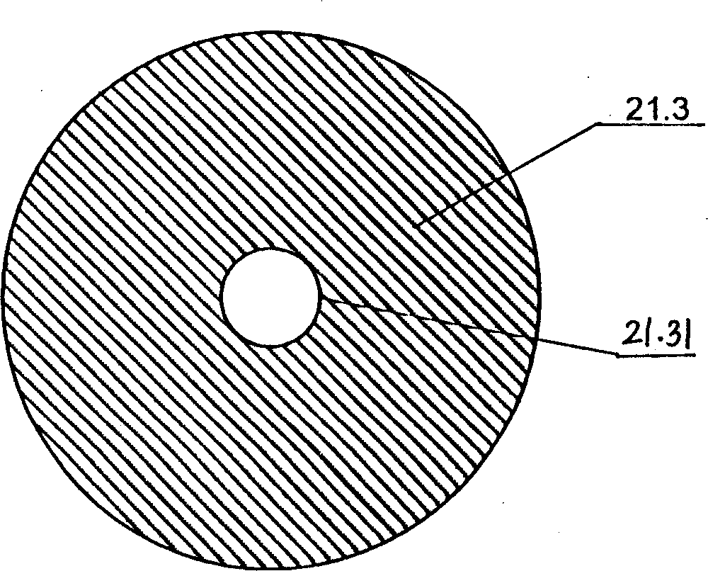
[0057] like Figure 2A , 2B As shown, the surface of the metal part 10 to be treated in the present invention is in a state of being subjected to external stress, and a fixing member 21 is used to fasten the metal part 10 . Its fixed part 21 is made up of a base plate 21.2, and the pressure plate flange joint 21.1 is installed on the base plate 21.2, and the metal part 10 is close to the protection cushion block 21.3 inserted between the part 10 and the base plate 21.2, and passes through the base plate 21.2 and the cushion block The through hole A21.21 of 21.3 and a rod 21.4 of B21.31 apply a force to the metal part 10 fixed by the flange 21.2. The through hole A21.21 is provided ...
Embodiment 3
[0061] The difference from Example 1 is:
[0062] The present invention is achievable in combination with external mechanical stress and / or heat treatment to achieve the desired results on the surface. In order to facilitate the fragmentation of crystal grains located in the deep layer of the material, the present invention can also adopt the method of applying external mechanical stress and / or increasing the temperature, so that the deep layer of the material is more likely to produce plastic deformation in all directions.
[0063] The implementation results show that:
[0064] Surface processing is carried out on the metal part 10 in the state of no external mechanical stress. The experimental results of the present invention have obtained a nanostructure surface layer with a thickness of 20 μm, and can obtain hundreds of microns (or larger) under the state of external stress and / or heating. thick nanostructured surface layer. It is possible to achieve an increase in the t...
PUM
| Property | Measurement | Unit |
|---|---|---|
| Thickness | aaaaa | aaaaa |
| Thickness | aaaaa | aaaaa |
| Thickness | aaaaa | aaaaa |
Abstract
Description
Claims
Application Information


