

Organic electroluminescent device and its prepn.
An electroluminescence device and electroluminescence technology, which can be applied to electroluminescence light sources, electric light sources, electrical components, etc., and can solve the problems of inapplicability to small molecule OLED devices and the complexity of the preparation process.
- Summary
- Abstract
- Description
- Claims
- Application Information
AI Technical Summary
Problems solved by technology
Method used
Image

Examples
Embodiment 1
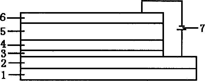
[0031] The ITO glass with a sheet resistance of 70Ω was cleaned and dried by boiling detergent and ultrasonic deionized water, and the film thickness of ITO was 100nm. Put the cleaned ITO glass under a pressure of 1×10 -3In a vacuum chamber of Pa, a Teflon buffer film was evaporated on the ITO film by thermal evaporation, the evaporation rate was 0.04nm / s, and the film thickness was 2nm. On the Teflon buffer film, continue to vapor-deposit the hole transport layer NPB, the vapor deposition rate is 0.4nm / s, and the film thickness is 40nm. Continue to vapor-deposit organic functional layer Zn(Ac) on the NPB layer 2 , the evaporation rate is 0.2nm / s, and the film thickness is 60nm. In Zn(Ac) 2 The metal layer is continuously vapor-deposited on the layer, and the metal layer is sequentially composed of Mg-Ag alloy and Ag. The total evaporation rate of Mg-Ag is 1.5nm / s, and the ratio of Mg and Ag evaporation rates is 4:1. The film thickness is 100nm; the evaporation rate of Ag ...
Embodiment 2
[0033] The ITO glass with a square resistance of 60 Ω was cleaned and dried by boiling detergent and ultrasonic deionized water, and the film thickness of ITO was 180 nm. Put the cleaned ITO glass under a pressure of 1×10 -4 In the vacuum chamber of Pa, a Teflon buffer film was deposited on the ITO film by thermal evaporation method, the evaporation rate was 0.02nm / s, and the film thickness was 1nm. The hole transport layer TPD is continuously evaporated on the Teflon buffer film, the evaporation rate is 0.2nm / s, and the film thickness is 40nm. Continue to vapor-deposit the organic functional layer Alq on the TPD layer 3 , the evaporation rate is 0.1nm / s, and the film thickness is 60nm. in Alq 3 The metal layer is continuously evaporated on the layer, and the metal layer is composed of Ca and Ag in turn. The evaporation rates of Ca and Ag are 0.6nm / s and 0.3nm / s respectively, and the film thicknesses are 35nm and 130nm respectively. The lighting voltage of the device is 2....
Embodiment 3
[0035] The ITO glass with a sheet resistance of 30Ω was cleaned and dried by boiling detergent and ultrasonic deionized water, and the film thickness of ITO was 240nm. Put the cleaned ITO glass under a pressure of 1×10 -5 In the vacuum chamber of Pa, a Teflon buffer film was deposited on the ITO film by thermal evaporation method, the evaporation rate was 0.01nm / s, and the film thickness was 6nm. On the Teflon buffer film, the hole transport layer MTDATA was continuously evaporated, the evaporation rate was 0.2nm / s, and the film thickness was 40nm. Continue to vapor-deposit organic functional layer Zn(Ac) on top of MTDATA layer 2 , the evaporation rate is 0.2nm / s, and the film thickness is 40nm. In Zn(Ac) 2 The metal layer is continuously evaporated on the layer, and the metal layer is composed of Ca and Ag in turn. The evaporation rates of Ca and Ag are 0.8nm / s and 0.2nm / s respectively, and the film thicknesses are 25nm and 150nm respectively. The lighting voltage of the ...
PUM
 Abstract
Description
Claims
Application Information