Design method of plane light delay device and its structure

A design method and delayer technology, applied in the field of optical communication, can solve problems such as impracticality and transmission rate limitation, and achieve the effects of wide spectrum range, good delay, and broad application prospects

Inactive Publication Date: 2002-09-04
FUDAN UNIV
View PDF0 Cites 1 Cited by
  • Summary
  • Abstract
  • Description
  • Claims
  • Application Information

AI Technical Summary

Problems solved by technology

Recently Zhu et al. have studied the use of defective one-dimensional photonic crystals as optical retarders (Time delay of light propagation through defect modes of one-dimensional photonic band-gap structures, Shi-yao Zhu et al., Optics Communications 174(2000) 139- 144, 15 January 2000), but this kind of delay can only be used in a narrow spectrum range, so its transmission rate is greatly limited
so they are not practical for high-speed optical communication

Method used


Image

  • Design method of plane light delay device and its structure
  • Design method of plane light delay device and its structure
  • Design method of plane light delay device and its structure

Examples


Embodiment 1

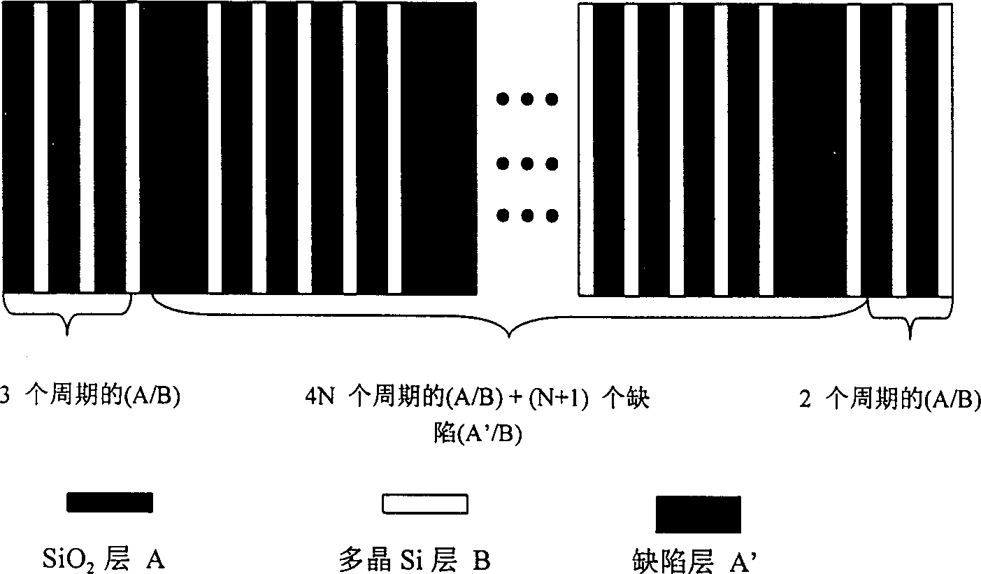
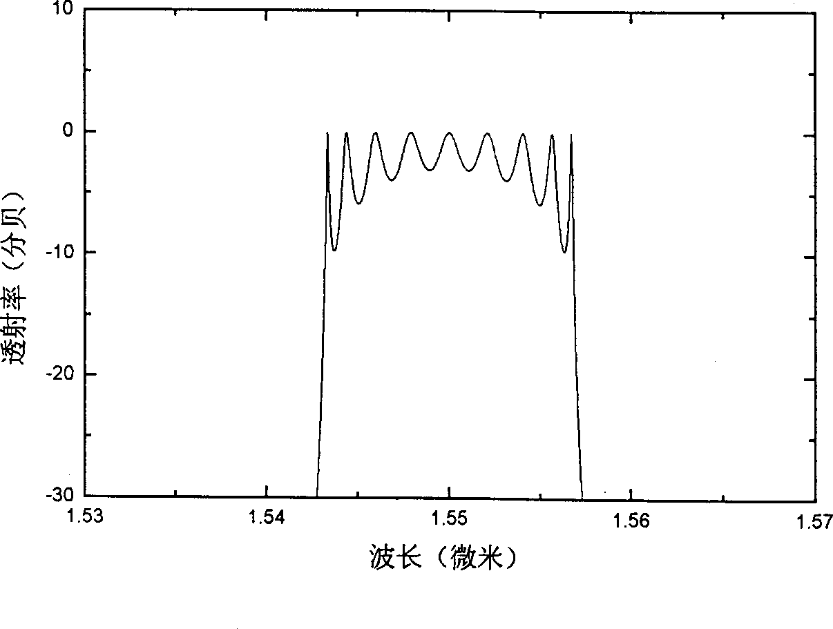
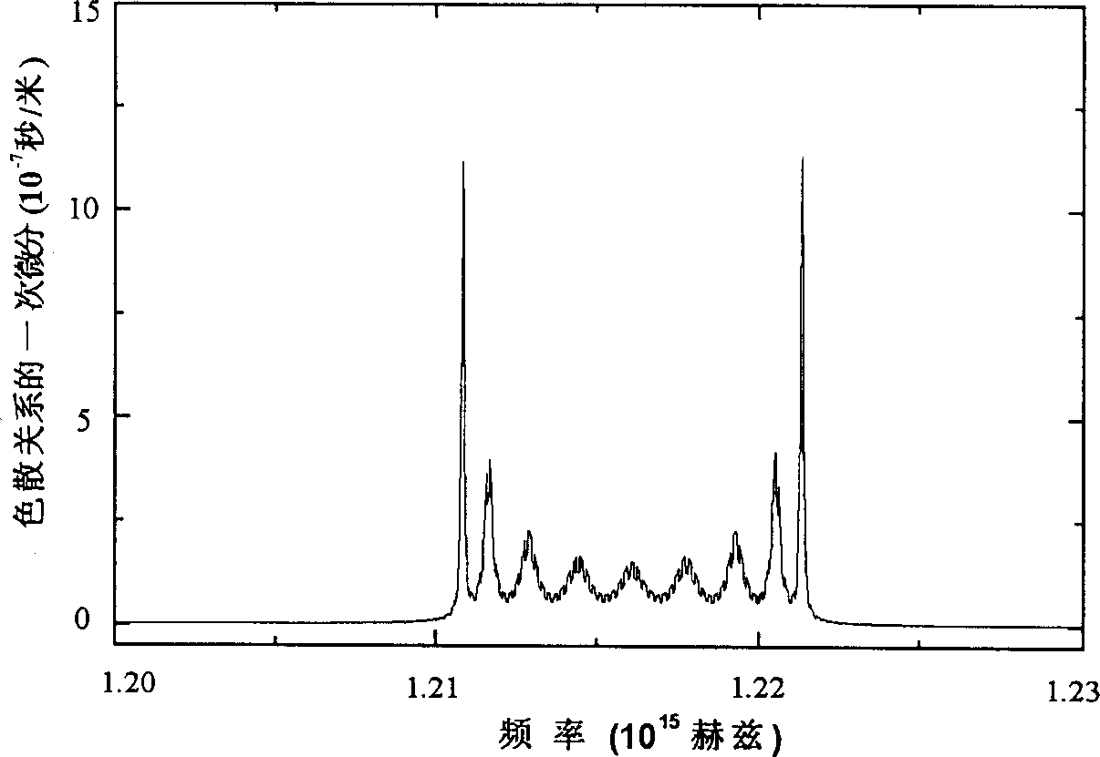
[0018] The preset operating wavelength of embodiment 1 is 1.55 μm, where polycrystalline Si and amorphous SiO 2 The refractive indices are 3.5 and 1.45, respectively. The thicknesses are 0.111 μm and 0.267 μm respectively, the left and right ends of the structure are taken as 2 and 3 normal structural periods respectively, N is taken as 9, and the defect layer of amorphous SiO 2 The thickness is taken as 0.534 μm. The transmission spectrum of the film system calculated by the transmission matrix method is as follows figure 2 As shown, the first differential of the dispersion relation is as image 3 shown. It can be seen from the figure that the retarder of this structure can reduce the speed of light to 1×10 7 m / s, the applicable spectrum range Δω is 8×10 12 Hertz can meet the basic requirements of high-speed optical communication.

Embodiment 2

[0019] Example 2 is similar to Example 1, for the working wavelength of 1.3 μm, select polycrystalline Si and amorphous SiO 2 The thicknesses are 0.093 μm and 0.224 μm respectively, the left and right ends of the structure are taken as 2 and 3 normal structure periods respectively, N is taken as 11, and the defect layer of amorphous SiO 2 The thickness is taken as 0.448 μm. The calculation and simulation results show that the optical retarder has good retardation and wide spectrum range under this parameter condition.


PUM

PropertyMeasurementUnit
thicknessaaaaaaaaaa
thicknessaaaaaaaaaa

Abstract

The present injvention belongs to the field of optical communication technology. According to the intercoupling theory between photon crystal defect states said invention researches the relationshipobetween defect layer thickness and transmission spectrum, relationship between number of periods of structure between defect layers and transmission spectrum and influence of defect with different quantitites to the performance of device so as to design the invented plane optical delay device. Said invneted plane optical delay device is characterized by that several defect states can be introduced into polycrystal Si / noncrystal SiO2 multilayer membrane, and the intercoupling between defect states can be used to broaden the transmission spectrum of device and can meet the basic requirements ofhigh-speed optical communication.

Description

technical field [0001] The invention belongs to the technical field of optical communication, and in particular relates to a design method and structure of a planar optical retarder. Background technique [0002] With the rapid development of information and communication technology, optical retarders have been widely used in many aspects such as optical signal processing and optical communication. Photonic crystals have been proven to be a suitable material for optical retarders. The photonic crystals that have been reported as optical retarders are: Scalora et al. reported for the first time that a one-dimensional photonic crystal with 30 cycles was used as an optical retarder, which can reduce the speed of light to 1.67×10 7 m / s (Ultrashort pulse propagation at the photonic band edge: Large tunable group delay with minimal distortion and loss, M. Scalora et al., PHYSICAL REVIEW E VOLUME 54, NUMBER2, AUGUST 1996). Recently, Zhu et al. studied the use of defective one-dim...

Claims


Application Information

Patent Timeline
Patent Type & Authority Applications(China)
IPC IPC(8): G02B6/12G02B6/28G02F1/03
Inventor 刘坚施斌樊永良赵登涛蒋最敏王迅
Owner FUDAN UNIV
Why Eureka
Try Eureka