High speed and high-capacity flash solid memory structure and manufacture process

A solid-state memory, high-capacity technology, applied in the field of electronic information, which can solve the problems of slow storage speed and insufficient storage capacity.

Inactive Publication Date: 2002-10-23
INST OF ELECTRONICS NO 15 MINIST OF INFORMATION IND
View PDF0 Cites 6 Cited by
  • Summary
  • Abstract
  • Description
  • Claims
  • Application Information

AI Technical Summary

Problems solved by technology

[0005] In order to overcome many defects of the existing solid-state memory such as slow storage speed and insufficient storage capacity, a solid-state memory with fast storage speed and large capacity is newly developed.

Method used


Image

  • High speed and high-capacity flash solid memory structure and manufacture process
  • High speed and high-capacity flash solid memory structure and manufacture process
  • High speed and high-capacity flash solid memory structure and manufacture process

Examples


Embodiment Construction

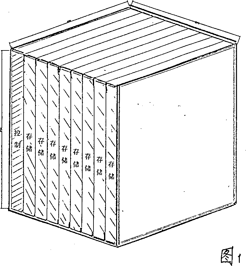
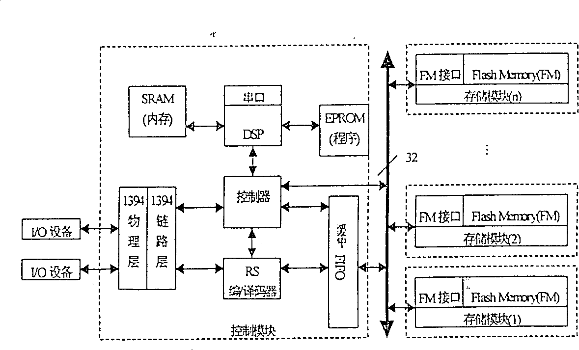
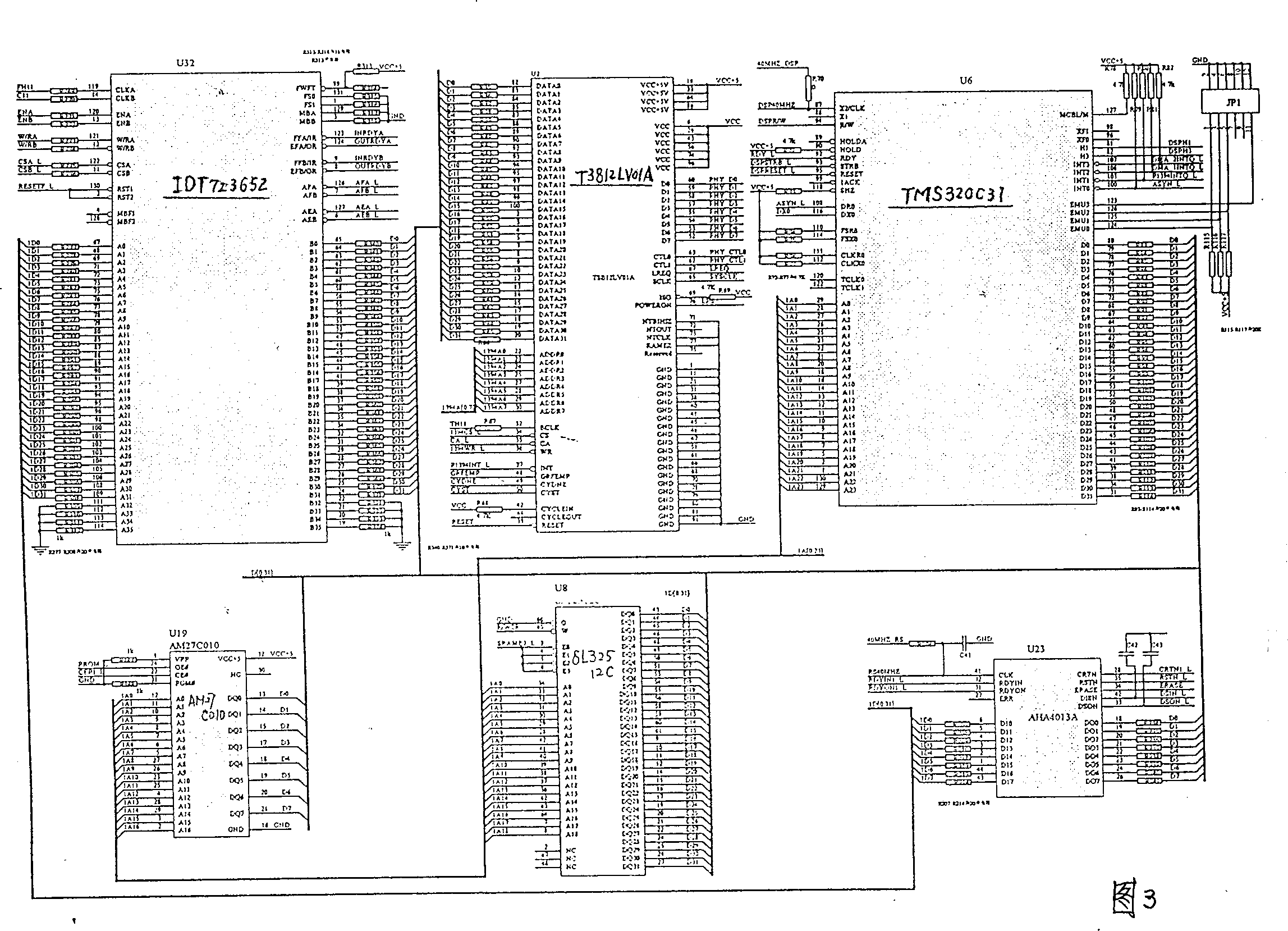
[0012] Referring to Fig. 1, it shows the schematic diagram of the building block stacked structure of the solid-state memory, in the present embodiment, 8 storage bodies are stacked together to form a high-speed large-capacity flash solid-state memory, figure 2 A block diagram showing that the memory is composed of a control module and a storage module, wherein the control module includes the data receiving / sending part, data verification and data buffering, which consists of DSP, controller, 1394 interface, RS encoder / decoder, buffering FIFO, EPROM to store programs and SRAM to store data. Among them, the DSP adopts 32bits TMS320C3X, the controller is realized by a programmable chip (ISPLS2192VE), and the input / output selects a device conforming to the IEEE 1394-1995 standard (the physical layer uses TSB41LV03 three-port cable receiver / transmitter, and the link layer uses TSB12LV01A high-speed serial Bus link layer controller), error correction and error detection use the RS ...


PUM


Abstract

This invention relates to a flash solid memory structure containing a controlling module and multi-memory modules related to the storage memory volume with a modular laminated structure adopting uneasy to be lost FLASH memory chips as the medium. The controlling module with DSP as the center consists of programmable chip control circuit, interface 1394, RS coder-decoder, buffer FIFO, EPROM of storing program chip and SRAM of storing data chip. The process of the storage memory is as the following two steps of writing in the storage memory chips: a. Data write-in: writing data into the page registers by ns, b. Automatically program: transmitting the data of the page registers to the memory unit, the above two steps should be taken by turns so as to greatly reduce the write-in time comparing with ordinary multi-route parallel write-in technology.

Description

(1) Technical field [0001] The invention belongs to the technical field of electronic information, and in particular relates to a high-speed and large-capacity flash solid-state storage device. (2) Background technology [0002] As one of the important components of the computer system, the memory can be regarded as a warehouse for storing data outside the computer. In the prior art, the main external memory includes soft and hard disk drives, magnetic tape drives, and optical disk drives. The mechanism of storing data on the magnetic layer has different characteristics and is used in different occasions only because of the different media (or media) for storing data and different structures. However, these memories cannot get rid of the weakness of magnetic media. They are affected by the environment. The impact of temperature is large, and it cannot withstand mechanical vibration and shock. As a memory, its storage capacity and speed are greatly limited, which affects its ...

Claims


Application Information

Patent Timeline
Patent Type & Authority Applications(China)
IPC IPC(8): G06F12/00G11C11/34H01L21/50H01L21/98H01L25/10H01L27/10
Inventor 徐军王茂鸿耿殿品陈济民赵秋云高颖芝刘蕊王耀中余锦肖燕王景华王士成王钧
Owner INST OF ELECTRONICS NO 15 MINIST OF INFORMATION IND
Why Eureka
Try Eureka