Semiconductor device

A technology of semiconductors and devices, applied in the field of DC-DC converters, can solve the problems that the rectifier device Q10 cannot be completely prevented from being turned on

Inactive Publication Date: 2002-11-06
TDK CORPARATION
View PDF1 Cites 10 Cited by
  • Summary
  • Abstract
  • Description
  • Claims
  • Application Information

AI Technical Summary

Problems solved by technology

[0009] Therefore, it is impossible to completely prevent the rectifier device Q10 that should be turned off from entering the on state (self-conducting state).

Method used


Image

  • Semiconductor device
  • Semiconductor device
  • Semiconductor device

Examples


Embodiment Construction

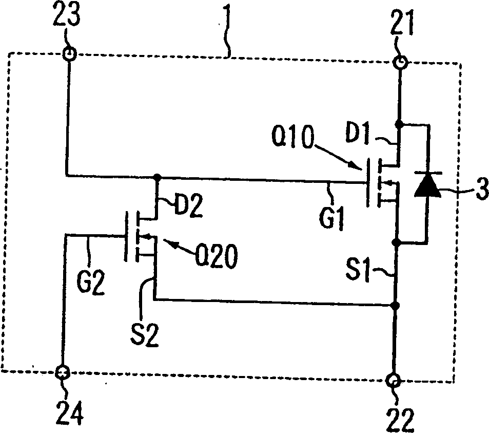
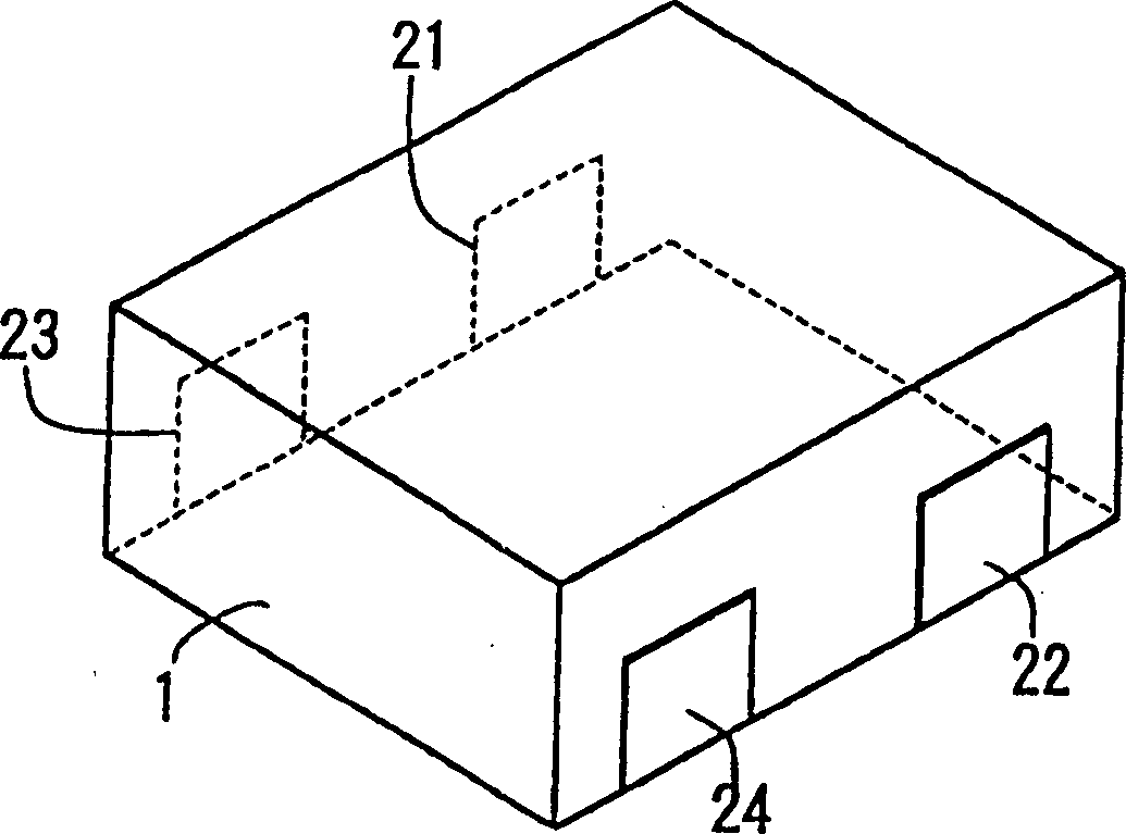
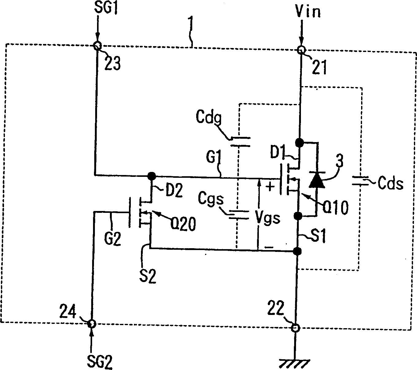
[0024] figure 1 An equivalent circuit and a general configuration of a semiconductor device according to the present invention are shown. The illustrated semiconductor device includes a first FET Q10 , a second FET Q20 , and a package 1 . The first FET Q10 and the second FET Q20 are in the package 1 . The first FET Q10 constitutes a main switch. The drain D2 and source S2 of the second FET Q20 are connected to the gate G1 and source S1 of the first FET Q10. The outer surface of the package 1 has terminals of the first and second FETs Q10 and Q20. In the illustrated embodiment, the first FET Q10 and the second FET Q20 comprise a single chip. That is, the first FET Q10 and the second FET Q20 are formed on the same silicon substrate.

[0025] In the first FET Q10 , the gate G1 is connected to the external terminal 23 , the drain D1 is connected to the external terminal 21 , and the source S1 is connected to the external terminal 22 . The gate G2 of the second FET Q20 is co...


PUM


Abstract

A semiconductor device capable of short-circuiting a gate-source capacitance of a FET (Field Effect Transistor) as a main switching device with low impedance is proposed. The above semiconductor device includes a first FET, a second FET, and a package. Both the first FET and the second FET are contained within the package. The first FET constitutes a main switching device. The drain and source of the second FET are connected to the gate and source of the first FET. An outer surface of the package has external terminals of the first and second FETs.

Description

technical field [0001] The present invention relates to a semiconductor device using a plurality of field effect transistors (hereinafter referred to as FETs) and a DC-DC (direct current-direct current) converter using the semiconductor device in a synchronous rectifier circuit. Background technique [0002] High-speed output rectifier diodes have been used in rectifier devices of DC-DC converters. Due to its lower output voltage and higher current, the forward voltage drop of the diode can no longer be ignored. As a countermeasure against this problem, a so-called synchronous rectifier circuit system has been proposed and put into practice, which utilizes a switching device such as a FET to provide a small voltage drop in the on state. [0003] When FETs are used in the rectification device of the synchronous rectifier circuit, because the control is realized by the voltage between the gate and the source, malfunctions may occur, especially in the non-conduction (OFF) stat...

Claims


Application Information

Patent Timeline
Patent Type & Authority Applications(China)
IPC IPC(8): H01L27/04H01L21/822H01L21/8234H01L27/088H02M3/155H02M7/21H03K17/0412H03K17/16H03K17/687
CPCH03K17/162H02M3/155H03K17/04123
Inventor 广川正彦松浦研高木雅和
Owner TDK CORPARATION
Why Eureka
Try Eureka