Method for hermetic sealing of electronic parts

A technology for airtight sealing and electronic components, which is applied in electrical components, electric solid devices, circuits, etc., and can solve problems such as difficulty in airtight sealing

Inactive Publication Date: 2003-01-29
TANAKA PRECIOUS METAL IND
View PDF0 Cites 5 Cited by
  • Summary
  • Abstract
  • Description
  • Claims
  • Application Information

AI Technical Summary

Problems solved by technology

However, as electronic components are miniaturized to me

Method used


Image

  • Method for hermetic sealing of electronic parts
  • Method for hermetic sealing of electronic parts
  • Method for hermetic sealing of electronic parts

Examples


Embodiment

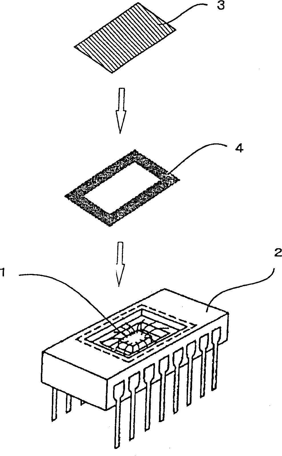
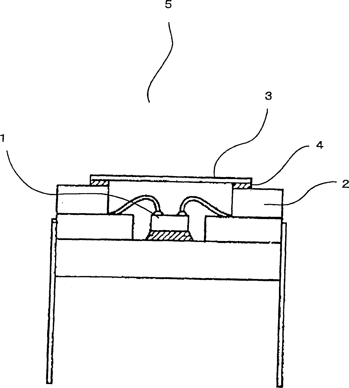
[0026] The ingot of 78.5% by weight of Au-21.5% by weight of Sn made by the fusion casting method is rolled into a sheet, and then a square ring-shaped solder is formed by punching. Next, the cover is joined to the base on which the IC chip is mounted with this solder, and an IC package is made. Such as figure 1 As shown, after the above processing, the solder 4 is sandwiched between the ceramic base 2 with IC1 and the Kovar cap 3 plated with Au beforehand, and they are heated to 300°C in a conveyor heating furnace to make the solder 4 The IC package 5 is formed by melting and joining. The cross-sectional view of the IC package after bonding at this time is shown in figure 2 .

Embodiment 1

[0030] (Measurement of leakage rate)

[0031] The IC packages produced in the above embodiments and comparative examples were subjected to a helium leak test as a fine leak test. Compare and check the leakage rate of IC packages manufactured by the two. The helium leak test is carried out by placing the manufactured IC package on the helium leak detector, and leaking the internal helium molecules by drawing a vacuum outside the IC package, and calculating the leaked helium molecules.

[0032] As a result, the leakage rate (unseal rate) of the IC package using the solder material of 80% by weight of Au-20% by weight of Sn of the comparative example was 0.2%. In contrast, the leakage rate of the IC package manufactured in this embodiment is 0.1%, and it is confirmed that it can improve the leakage rate more than the airtight sealing method of the comparative example.

Embodiment 2

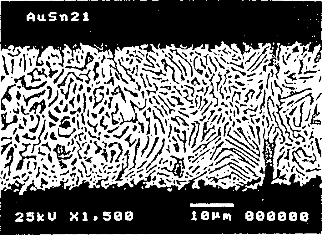
[0034] (Observation of joint tissue)

[0035]Then, in order to confirm the structure of the bonding part (solder layer) of the IC package produced in the embodiment and the comparative example, both bonding parts were observed with SEM (Scanning Electron Microscope). The SEM photographs of the joints of the embodiment and the comparative example are shown in image 3 with Figure 4 . From these SEM photographs, it was confirmed that the joint portion of the present embodiment has a fine eutectic structure. On the other hand, it was confirmed that there is a coarse Au-rich phase ( Figure 4 The white part in). Since the size of these Au-rich phases is different, it is considered that the thickness of the solder layer at the time of joining is slightly uneven, which may cause leakage.


PUM


Abstract

There is provided a method of hermetically sealing electronic parts, comprising the step of bonding a base having semiconductor devices mounted thereon and a cap together via a solder. The solder is composed, by weight, of 78% or more but less than 79.5% Au, and the balance Sn. It is particularly preferred that the bonding is performed with the use of a solder composition composed, by weight, of 78% or more but 79% or less Au, and the balance Sn as the solder and furthermore through plating the cap with gold.

Description

Technical field [0001] The present invention relates to a method for hermetic sealing of electronic components in which a container (base) containing semiconductor components and a cover are joined by solder. In particular, it relates to an airtight sealing method in which the leakage occurrence rate can be reduced to not more than 1 / 10 of the previous method. Background technique [0002] When various semiconductor components such as SAW filters and quartz crystal resonators are in their own state, there is a possibility that the conductive lattice and gaskets will corrode and the characteristics will deteriorate due to oxygen and moisture in the air. Therefore, in order to completely isolate the semiconductor components from the outside air, the internal vacuum is usually hermetically sealed or filled with He or N 2 The semiconductor element is mounted on the electronic device in the state of the metal or ceramic container (package). [0003] Here, as the hermetic sealing techn...

Claims


Application Information

Patent Timeline
IPC IPC(8): B23K35/26B23K35/30H01L21/50H01L23/10
CPCH01L21/50H01L2924/16195H01L2924/15153H01L23/10B23K35/3013H01L24/48H01L2924/01079H01L2224/48465H01L2224/48227H01L2924/1517H01L2924/01322H01L2924/01327H01L24/49H01L2924/01078B23K2201/36H01L2224/48091H01L2224/49171H01L2224/73265H01L2924/166H01L2224/32225H01L2924/12042H01L2224/05599H01L2224/85399H01L2924/00014B23K2101/36H01L2924/00H01L2224/45099H01L2224/45015H01L2924/207
Inventor 岩井正三郎小林胜泽田治
Owner TANAKA PRECIOUS METAL IND
Why Eureka
Try Eureka