Eureka AIR delivers breakthrough ideas for toughest innovation challenges, trusted by R&D personnel around the world.

Prepn of nitride-oxide film

A technology of oxide film and pre-oxidation, which is used in semiconductor/solid-state device manufacturing, electrical components, circuits, etc., and can solve problems such as inability to apply

Inactive Publication Date: 2003-03-19
SEMICON MFG INT (SHANGHAI) CORP +1
View PDF0 Cites 14 Cited by
  • Summary
  • Abstract
  • Description
  • Claims
  • Application Information

AI Technical Summary

Problems solved by technology

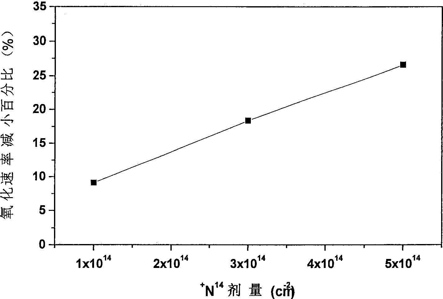
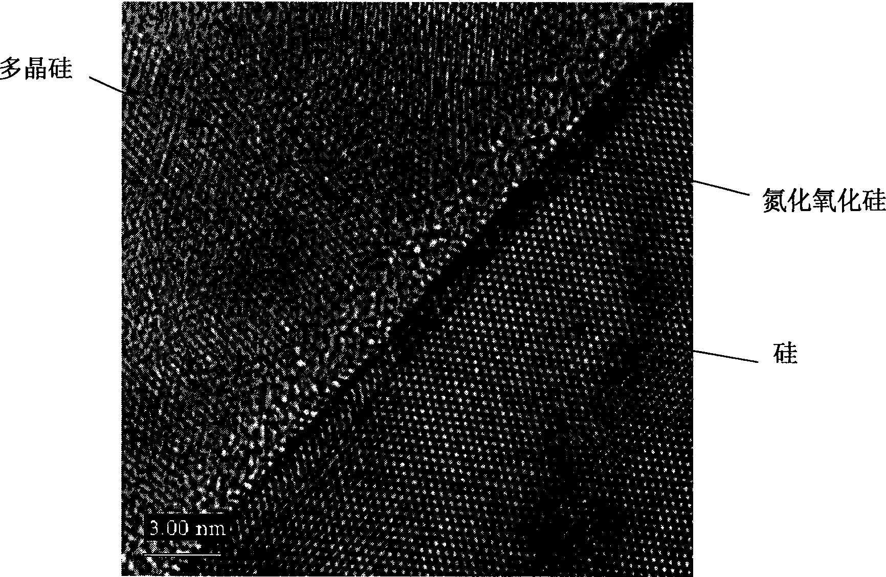
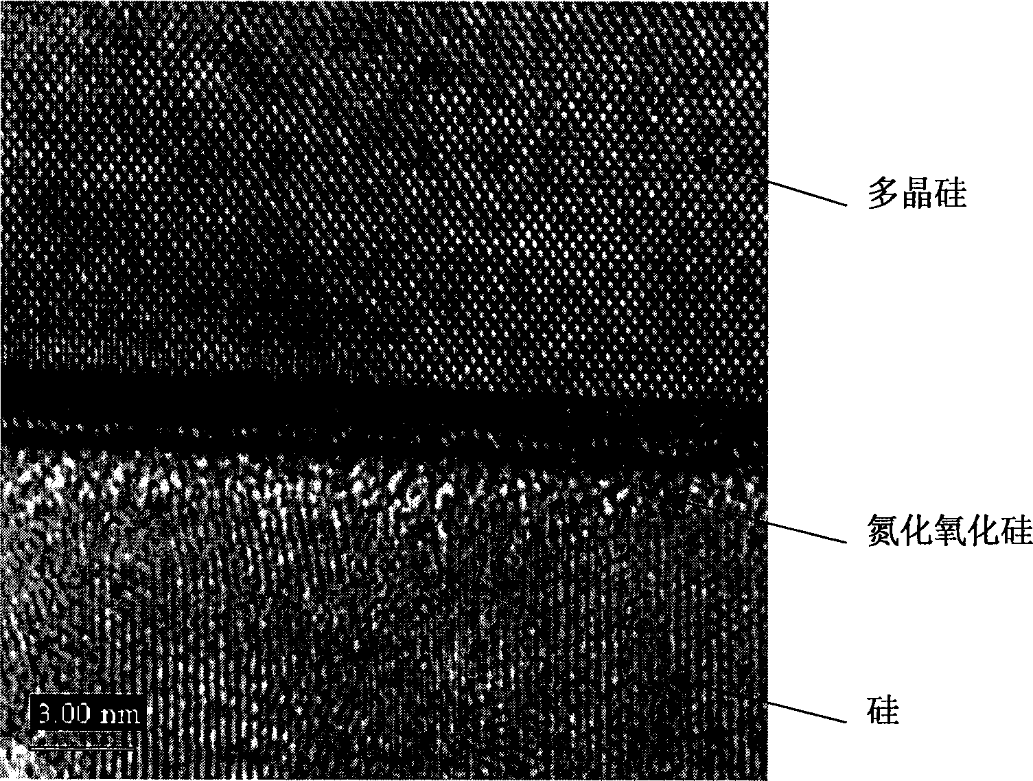
In order to overcome the problem that conventional nitrided oxide gate dielectrics cannot be applied to devices and circuits below 25 Å, the present invention first implants nitrogen ions into the silicon substrate, and then oxidizes

Method used


Image

  • Prepn of nitride-oxide film
  • Prepn of nitride-oxide film
  • Prepn of nitride-oxide film

Examples


Embodiment

[0026] Its formula of cleaning liquid that the present invention adopts is:

[0027] 3 # Liquid formula: H 2 SO 4 :H 2 o 2 =5:1 (volume ratio)

[0028] 1 # Liquid formula: NH 4 OH:H 2 o 2 :H 2 O=0.8:1:5 (volume ratio)

[0029] HF / IPA formula: HF:IPA:H 2 O=0.5%:0.02%:1

[0030] 1. Wafer cleaning: 3 # Liquid degumming for 10 minutes, 3 # Liquid cleaning 10 minutes, 1 # liquid wash for 5 minutes, H 2 O / HF (20 / 1) drift for 15 seconds.

[0031] 2. Pre-oxidation: thick 150 Å, 850 ℃, dry O 2 , 170 points+N 2 , annealed for 30 minutes.

[0032] 3. Chemical vapor deposition (LPCVD) Si 3 N 4 : Thickness 1300 Å, 780°C.

[0033] 4. Cleaning: 3 # solution for 10 minutes, 1 # Liquid 5 minutes, H 2 O / HF (1 / 20), drift for 15 seconds.

[0034] 5. Si 3 N 4 Annealing: 800°C, N 2 , annealed for 30 minutes.

[0035] 6. Photolithographic active area: 9912 glue, 1.2 μm.

[0036] 7. Reactive ion etching Si 3 N 4 : SiO is left in the active area 2 80 , power 150W, pr...


PUM


Abstract

The preparation of nitroxide film is to implant nitrogen ion into silicon substrate before oxidation. The steps includes: growing oxide film on isolated and cleaned silicon chip and implanting nitrogen ion to the active area; rinsing the oxide film; soaking with HF / IPA / H2O at room temperature and rinsing with deionized water before drying and feeding into furnace; feeding the boat slowly under protection of great flow rate of N2; heating to 700-900 deg.c and oxidation in N2 / O2 ratio of 5 for 1-120 min; annealing in N2 atmosphere at 700-900 deg.c for 15-60 min; lowing the temperature to 550 deg.c in N2 atmosphere and withdrawing the boat slowly under protecting of great flow rate of N2; forming polysilicon via LPCVD at 620 deg.c, 0.2 torr, SiH4 200 sccm and Ar 800 sccm.

Description

technical field [0001] The technology of the invention belongs to the field of microelectronic ultra-deep submicron CMOS devices and ultra-large-scale integration technology, and specifically relates to a preparation method of an ultra-thin nitrided oxide film, which is also applicable to the nitrided oxide film that needs to grow multiple thicknesses simultaneously on a chip. Preparation of oxide film. Background technique [0002] The goal of the current research on the basic technology of integrated circuits is to obtain higher unit integration, higher circuit speed, lower unit function power consumption and unit function cost. The main way to achieve the above goals is to continuously reduce (Scaling down) the CMOS technology of the device and wiring size, which is exactly what Moore's Law expresses. The current most advanced industrial CMOS technology has evolved to 0.13μm, and the laboratory has successfully prepared 20nm planar MOS devices and 18nm new structure MOS ...

Claims


Application Information

Patent Timeline
Patent Type & Authority Applications(China)
IPC IPC(8): H01L21/316H01L21/318H01L21/473
Inventor 徐秋霞侯瑞兵高文方韩郑生
Owner SEMICON MFG INT (SHANGHAI) CORP
Why Eureka
Eureka Blog
Learn More