Magnetic element and its manufacture, power supply module therewith

A technology of magnetic components and magnetic components, applied in the direction of inductance with magnetic core, inductance/transformer/magnet manufacturing, coil manufacturing, etc., can solve the problems of lack of mass production and high cost

Inactive Publication Date: 2003-04-02
PANASONIC CORP
View PDF10 Cites 30 Cited by
  • Summary
  • Abstract
  • Description
  • Claims
  • Application Information

AI Technical Summary

Problems solved by technology

[0008] The magnetic elements disclosed in the above publication need to be manufactured one by one or using vacuu

Method used


Image

  • Magnetic element and its manufacture, power supply module therewith
  • Magnetic element and its manufacture, power supply module therewith
  • Magnetic element and its manufacture, power supply module therewith

Examples


Embodiment 1

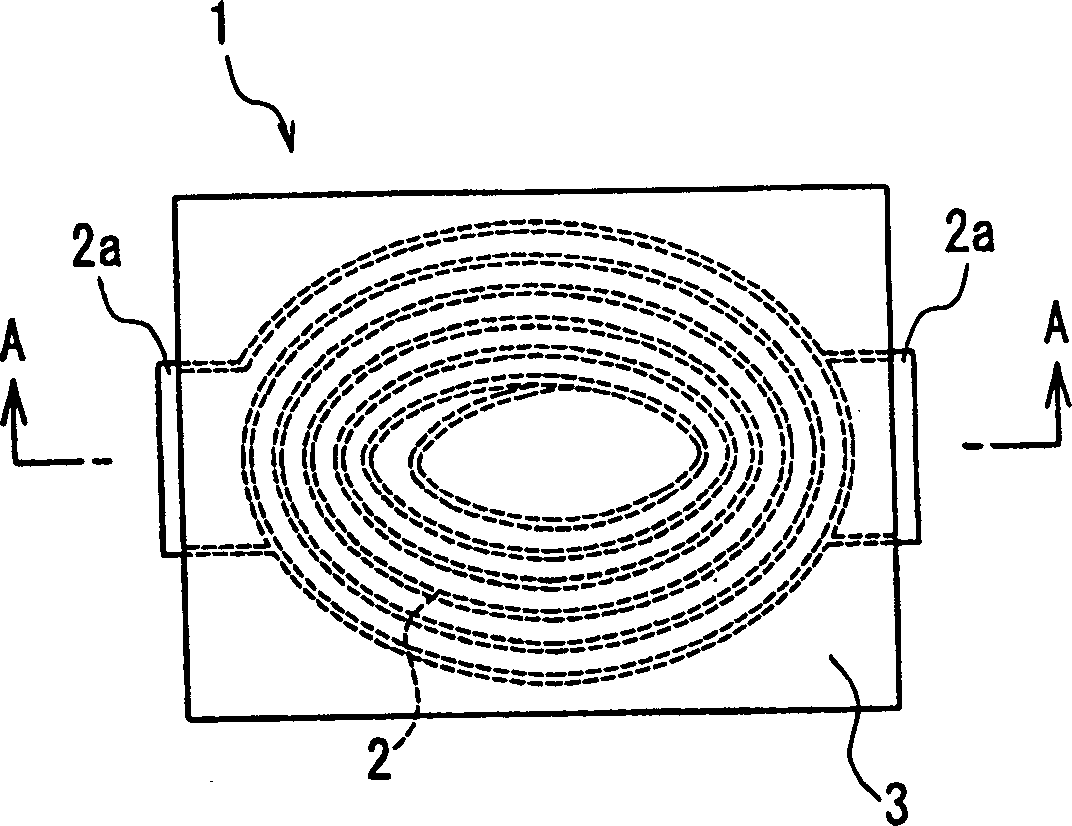
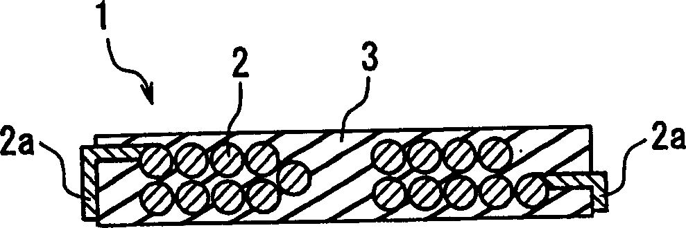
[0114] Two Fe-based amorphous thin bodies (METGLAS-26055C (manufactured by Hanewell Corporation, USA)) having a corner of 4 mm and a thickness of 20 μm were prepared as the first magnetic member 4 . As the second magnetic member 5, 14 wt. % After being made into a paste, shape it into a sheet with a doctor blade, heat and dry at 80° C. for 1 hour, and prepare a composite sheet with a thickness of about 310 μm. The chip coil 1 is a chip coil formed as follows: a tape with an outer diameter of 4.0mmφ, an inner diameter of 0.5mmφ, a thickness of 300μm, a conductor diameter of about 100μm, and a DC resistance of 170mΩ produced by an insulating material embedding plating method. Two stacked 18-turn conductor coils covered in insulation, formed into a sheet. The chip coil covers the conductor coil with an insulating substance having a lower magnetic permeability than the composite sheet used in the second magnetic member 5. In this embodiment, epoxy resin (based on bisphenol A) is ...

Embodiment 2

[0118] As the first magnetic member 4 , two MnZn-based ferrite sintered bodies with a length of 10 mm and a thickness of 0.5 mm were prepared. One of them was configured to have a protrusion with a diameter of 4.0 mm and a height of 0.6 mm at the center. In the same manner as in Example 1, an uncured composite sheet having a thickness of about 310 μm was prepared as the second magnetic member 5 . As the chip coil 1, a chip coil manufactured by an insulating material embedding plating method with an outer diameter of 7.5mmφ, an inner diameter of 4.5mmφ, a thickness of 600μm, a conductor diameter of about 250μm, and a DC resistance of 100mΩ is used. Two stacked coils of 14 turns of conductor with insulation covering, formed into sheet form. The insulating substance used is the same as in Example 1. Holes for fitting protrusions provided on the ferrite sintered body are provided at the center of the chip coil, and holes for arranging the second magnetic member 5 are provided at...

Embodiment 3

[0122] As the first magnetic member 4, a NiZn ferrite sintered body with a thickness of 0.2 mm was prepared. Prepare the second magnetic member 5 by mixing 16% by weight of epoxy-based curable resin (epoxy resin with bisphenol A as the main ingredient) in carbonyl (carbonyl) Fe powder with an average particle size of about 5 μm, and prepare a paste. . As the chip coil 1, a chip coil manufactured by an insulating material embedding plating method with an outer diameter of 2.8mmφ, an inner diameter of 0.8mmφ, a thickness of 250μm, a conductor diameter of about 100μm, and a DC resistance of 350mΩ is used. Two stacked coils of 16 turns of conductor with insulation covering, formed into sheet form. The insulating substance used is the same as in Example 1. In this embodiment, a large sheet forming a plurality of such sheet-like coils is prepared. The conductor coil has a structure in which its terminals are formed in the same plane, and its outer shape has a size of 3 mm×4 mm. ...


PUM

PropertyMeasurementUnit
Thicknessaaaaaaaaaa
Inductance valueaaaaaaaaaa
Dc resistanceaaaaaaaaaa

Abstract

A magnetic device includes a sheet-type coil including a planar conductive coil and an insulating substance; and a sheet-type first magnetic member disposed on at least one of upper and lower surfaces of the sheet-type coil, where a magnetic permeability of the insulating substance is smaller than a magnetic permeability of the first magnetic member. The magnetic device preferably includes a second magnetic member provided at a predetermined area of the sheet-type coil, the second magnetic member being made of a resin containing a magnetic powder and having a permeability larger than the insulating substance and smaller than the first magnetic member. The predetermined area is at least one position selected from a center portion and a peripheral portion of the sheet-type coil where a conductor constituting the planar conductive coil is not present. Further, a power supply module of the present invention includes the magnetic device according to the present invention.

Description

technical field [0001] The present invention relates to an inductor, a choke coil, a transformer, an ultra-thin magnetic element used therein, a manufacturing method thereof, and a power supply module equipped with the inductor, a choke coil, and a transformer of electronic equipment. Background technique [0002] In recent years, along with miniaturization and thinning of electronic equipment, there has been a strong demand for miniaturization and thinning of components and devices used therein, power supplies, and the like. In particular, in portable devices, there is a strong demand for thinning in addition to downsizing. On the other hand, LSIs such as CPUs have been speeded up and integrated, and a large current is supplied to a power supply circuit supplied by such LSIs. Therefore, in the magnetic element used in the inductor of such an LSI power supply circuit, it is necessary to reduce the resistance of the coil conductor to realize heat generation, and at the same ...

Claims


Application Information

Patent Timeline
IPC IPC(8): H01F3/10H01F17/00H01F17/04H01F27/32H01F41/00H01F41/04
CPCH01F27/327H01F17/04H01F17/0013H01F41/046H01F3/10H01F41/005Y10T29/4902
Inventor 井上修半田浩之
Owner PANASONIC CORP
Why Eureka
Try Eureka