Method for making DNA logic integrated circuit

A technology of deoxyribonucleic acid and integrated circuits, applied in circuits, semiconductor/solid-state device manufacturing, electrical components, etc., can solve problems that have never been mentioned before

Inactive Publication Date: 2003-04-23
陈柏瑞
View PDF0 Cites 0 Cited by
  • Summary
  • Abstract
  • Description
  • Claims
  • Application Information

AI Technical Summary

Problems solved by technology

[0007] The sequenced DNA sequence has already exceeded 3 billion pairs, and the dopant treatment method described in the present invention has been published in countless articles on medicine and biochemical engineering, and the method of depositing DNA on metal is even more innumerable. Enumeration, but no one has mentioned any method to adjust the conductive properties of DNA and the integration after doping treatment

Method used


Image

  • Method for making DNA logic integrated circuit
  • Method for making DNA logic integrated circuit
  • Method for making DNA logic integrated circuit

Examples


Embodiment

[0036] Device preparation and integration embodiment description

[0037] (1) DNA sample preparation:

[0038] 1. Single-stranded DNA was purchased from Perkin Elmer Taiwan Branch; pBR322-3A2 (18bp), pBR322-5S2 (18bp).

[0039] 2. Prepare double-stranded DNA by polymerizing chain reaction (PCR); use the commercial kit GeneAmp PCR Reagent Kit and Ber Taq DNA polymerase Kit to synthesize DNA.

[0040] 3. Alcohol precipitation method (using the principle of extremely low solubility of salts formed by DNA in alcohol to separate DNA from other impurities).

[0041] (1) Add 10-20 μL of 3.0 sodium acetate to 1ml of the solution and mix well.

[0042] (2) Add 1mL of 95% alcohol, mix well, and place at -20°C for about 30-40 minutes.

[0043] (3) Centrifuge at 13,000 rpm for 10 minutes at 4°C, and carefully remove the supernatant.

[0044] (4) Add 0.5 mL of ethanol to wash the DNA precipitate, centrifuge at 13,000 rpm at 4°C for 10 minutes, carefully remove the supernatant to obtai...


PUM


Abstract

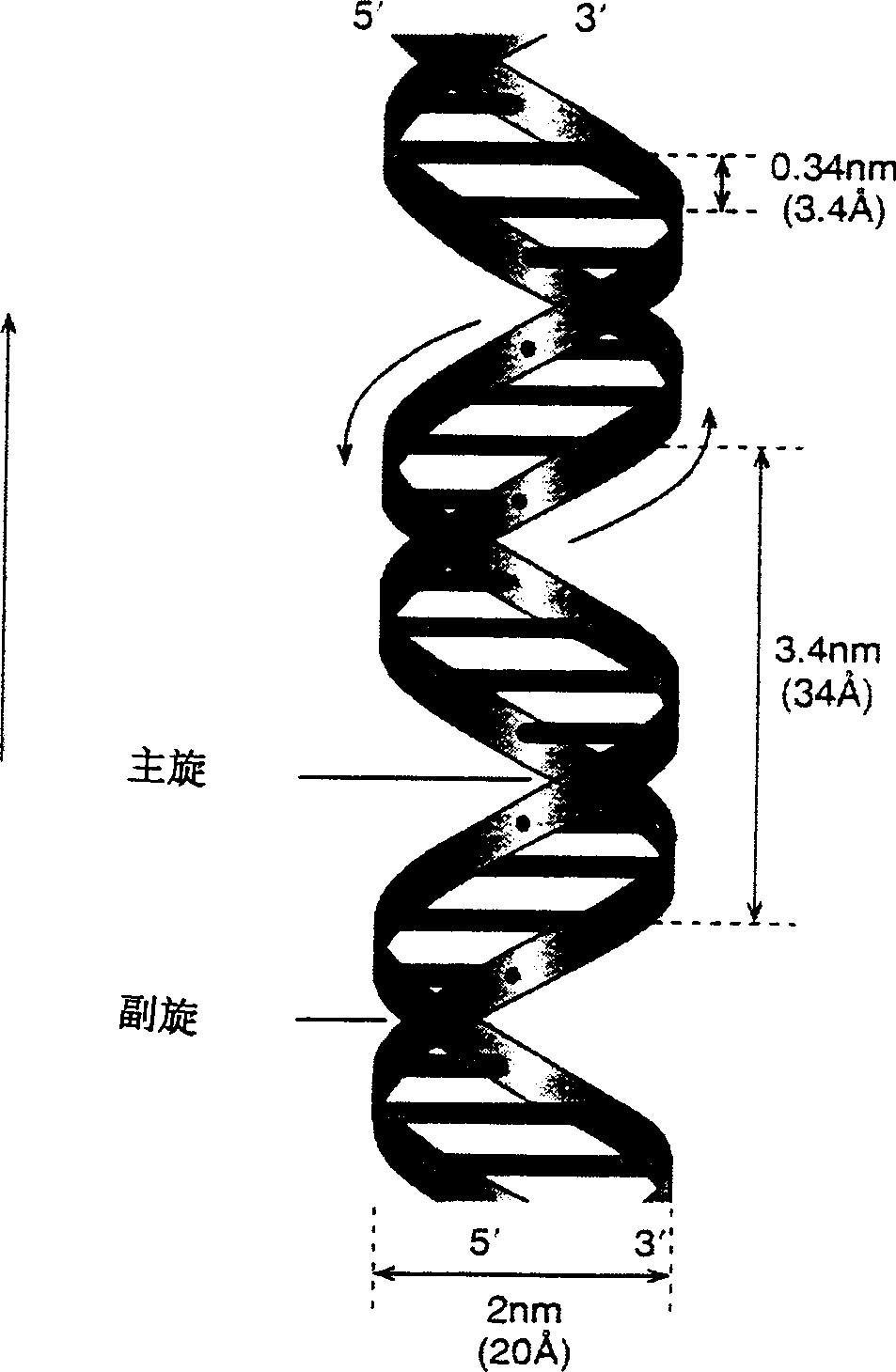
The present invention relates to a DNA logic integrated circuit and its production method. It uses double-chain DNA as substrate of semiconductor device, utilizes the DNA staining technique and mosaic principle of anticancer medicine and DNA between them to change energy gap of DNA molecule and further change the conductivity of DNA molecule. The diameter of DNA molecule is about 2 nm, and its minimum wire width is 2 nm only, and is far less than minimum wire width 0.13 micrometer (130 nm) of existent semiconductor technique, so that it does not use etching technique to make integrated circuit, and can make integrated circuit more miniature.

Description

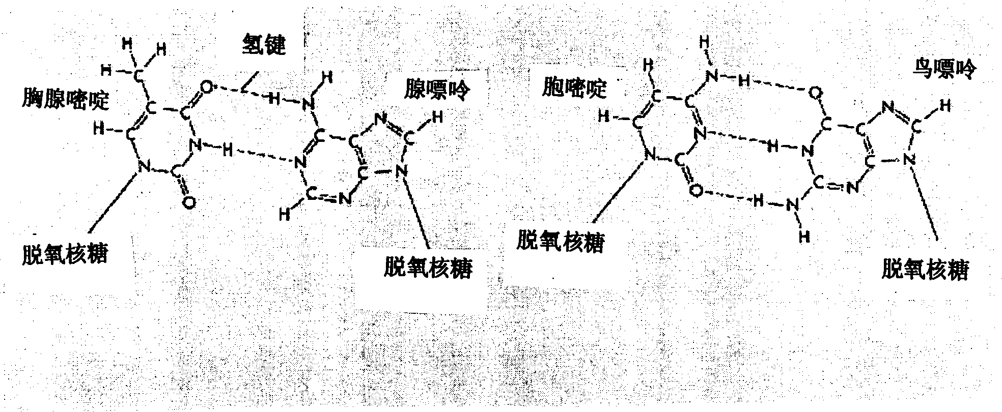
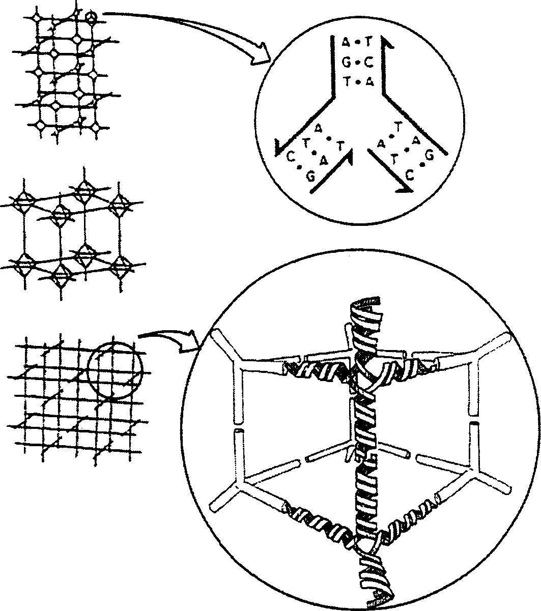
technical field [0001] The invention relates to a method for manufacturing a DNA integrated circuit. Using double-stranded DNA as the substrate of semiconductor devices, using DNA dyeing technology, mosaic between anticancer drugs and DNA and other principles to change the energy gap of DNA molecules, and then change the conductivity of DNA, and then use DNA fragments to link a single DNA Electronic devices, integrated into a DNA electronic device network. Background technique [0002] Integrated circuits (ICs, Integrated Circuits) are considered to be an inevitable trend after transistor technology reaches a certain stage of development. It is mainly a technology developed by J.Kilby and R.Noyce in 1959. Although the invention of the transistor replaced the bulky vacuum tube, the circuit can be reduced accordingly, but the wiring between electronic devices still depends on welding. way to achieve. When the circuit becomes larger and larger, the required soldering point r...

Claims


Application Information

Patent Timeline
Patent Type & Authority Applications(China)
IPC IPC(8): H01L21/70H01L31/0256
Inventor 陈柏瑞
Owner 陈柏瑞
Why Eureka
Try Eureka