Method of building crystal to grow lead zirconate titanate film
A lead zirconate titanate and thin film technology, which is applied in the directions of single crystal growth, crystal growth, single crystal growth, etc., can solve the problems of machine PZT thin film pollution and ferroelectric capacitor damage, etc.
- Summary
- Abstract
- Description
- Claims
- Application Information
AI Technical Summary
Problems solved by technology
Method used
Image
Examples
Embodiment Construction
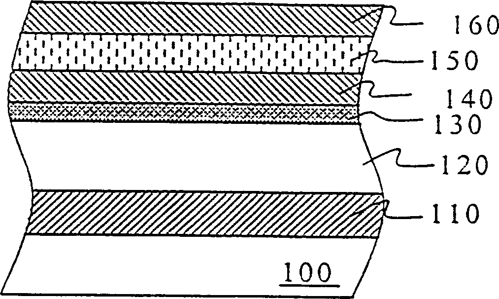
[0026] In this embodiment, the manufacturing process of the capacitor and the lead zirconate titanate film therein is taken as an example, wherein the lower electrode and the lead zirconate titanate film are formed by the method proposed in the present invention.
[0027] Please refer to figure 1 First, a dielectric layer 100 is provided, under which are CMOS components and other metal layers, and the uppermost metal interconnection structure 110 and a dielectric layer 120 have been formed on it, wherein the material of the dielectric layer 120 is preferably plasma Silicon oxide formed by volume-enhanced chemical vapor deposition (PECVD). Here, the reason why the metal interconnect structure 110 can be fabricated first is because the formation temperature of the lead zirconate titanate film of the present invention is relatively low as mentioned above.
[0028] Please continue to refer to figure 1 , and then deposit a barrier layer 130 on the dielectric layer 120, the materi...
PUM
 Abstract
Description
Claims
Application Information


