Method of mfg. integrated circuit with shallow junction

A technology of integrated circuits and shallow junctions, which can be used in circuits, semiconductor/solid-state device manufacturing, electrical components, etc., and can solve problems such as increasing doping concentration

Inactive Publication Date: 2003-05-07
ELECTRONICS & TELECOMM RES INST
View PDF0 Cites 5 Cited by
  • Summary
  • Abstract
  • Description
  • Claims
  • Application Information

AI Technical Summary

Problems solved by technology

The solid phase diffusion method is difficult to increase the doping concentration of the dopant in the solid phase diffusion source enough to make the shallow junction have low resistance
Moreover, there is the problem of precisely controlling the doping concentration of the dopant in the solid-phase diffusion source

Method used


Image

  • Method of mfg. integrated circuit with shallow junction
  • Method of mfg. integrated circuit with shallow junction
  • Method of mfg. integrated circuit with shallow junction

Examples


Embodiment Construction

[0018] Hereinafter, embodiments of the present invention will be described in detail with reference to the accompanying drawings. However, the embodiments of the present invention can be modified into various other forms, and the scope of the present invention is not necessarily limited to these embodiments. Moreover, these embodiments are provided to more fully explain the present invention to those of ordinary skill in the art. In the drawings, the thickness of layers or regions are exaggerated for clarity. Like reference numerals in the figures represent the same parts. Also, when it is written that a layer is formed "on" another layer or substrate, the layer may be formed directly on the other layer or substrate, or the other layer may be interposed therebetween.

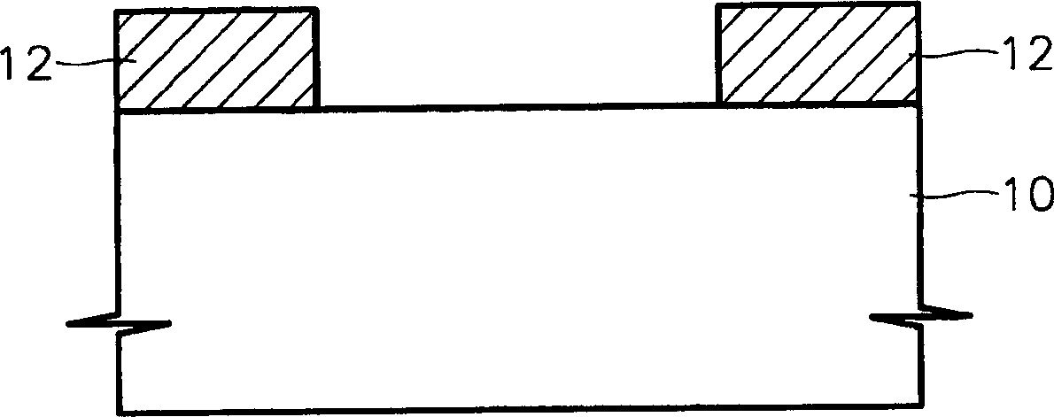
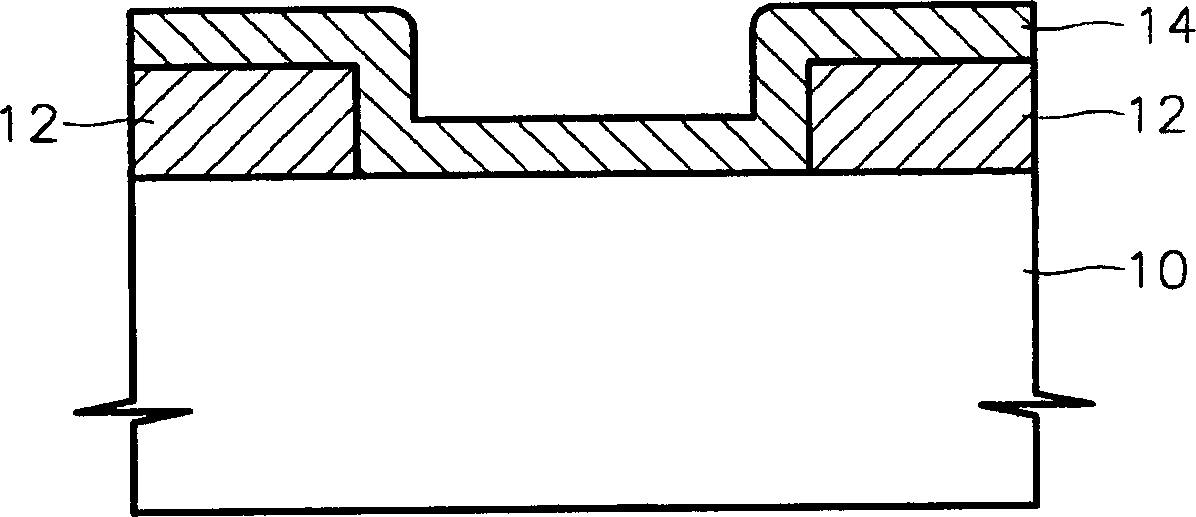
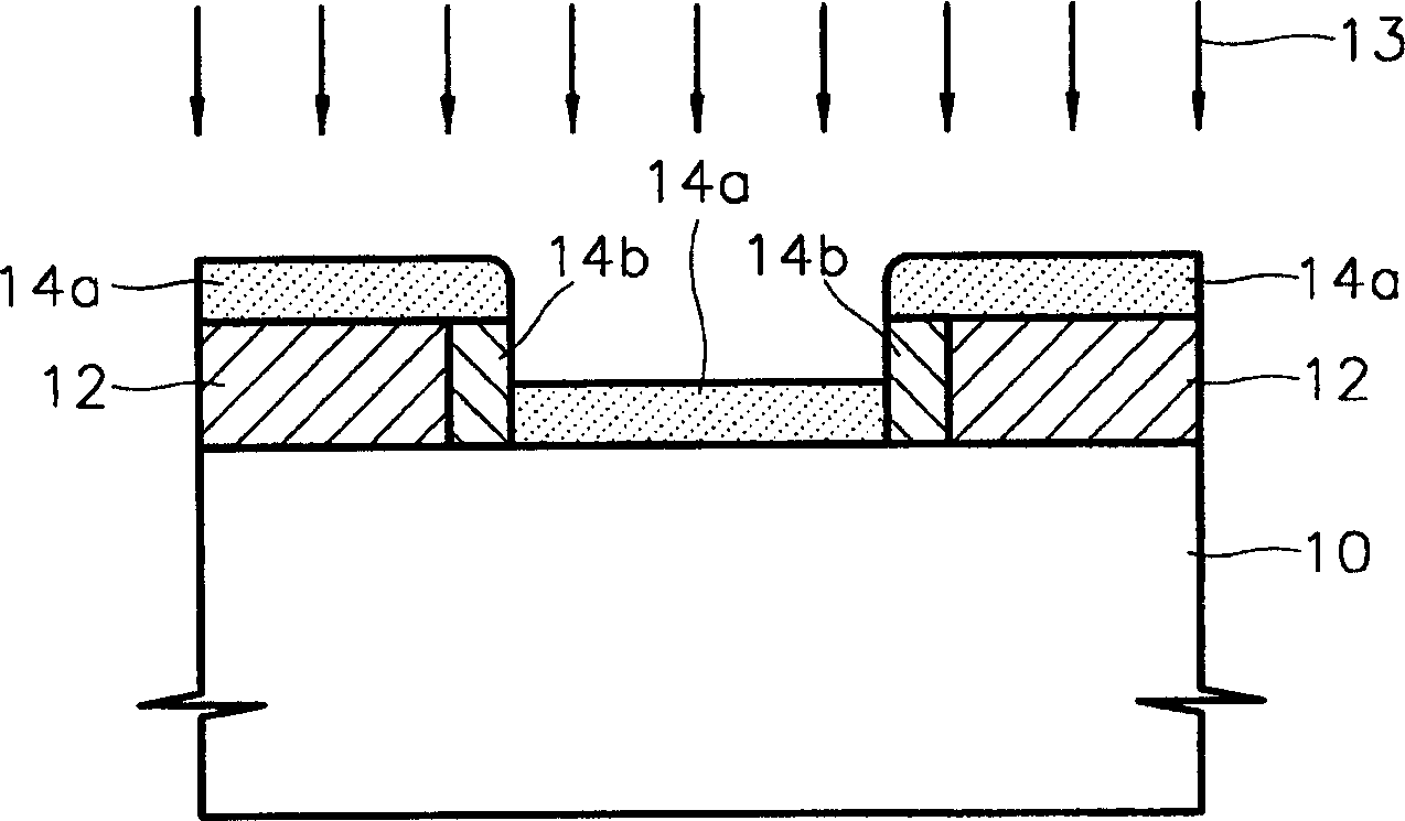
[0019] Figures 1 to 4 is a cross-sectional view illustrating a method of manufacturing an integrated circuit having a shallow junction according to a first embodiment of the present invention. see figure 1...


PUM

PropertyMeasurementUnit
Doping concentrationaaaaaaaaaa

Abstract

A method of fabricating an integrated circuit having shallow junctions is provided. A SOG layer containing impurities is formed on a semiconductor substrate. Impurity ions are additionally implanted into the SOG layer by a plasma ion implantation method to increase the concentration of impurities in the SOG layer. The impurity ions contained in the SOG layer having the increased concentration of impurities are rapidly heat-treated and diffused into the semiconductor substrate by a solid phase diffusion method to form shallow junctions. As a result, the concentration of impurities is precisely controlled by the plasma ion implantation method, and impurity ions are not directly implanted into the semiconductor substrate. Thus, the crystal structure of the semiconductor substrate is not damaged. Moreover, if the method of fabricating the integration circuit having the shallow junctions is applied after a gate electrode is formed, a LDD region and a highly doped source / drain region can be formed by a self-aligned method.

Description

technical field [0001] The present invention relates to a method of manufacturing integrated circuits, and more particularly to a method of manufacturing integrated circuits with shallow junctions. Background technique [0002] Generally, an integrated circuit (IC) is a group of discrete circuit devices including transistors, diodes, capacitors, resistors, etc. on a substrate, which are interconnected to perform specific functions in the circuit. IC can be divided into bipolar IC and MOS IC according to the type of transistor used. Bipolar ICs use n-p-n transistors or p-n-p transistors, while MOS ICs use metal oxide silicon (MOS) transistors. [0003] When an IC, especially a MOS IC, is highly integrated, it requires a shallow junction. A shallow junction is a junction that forms a shallow depth within the substrate, has a high concentration and high activation rate dopant, and has an abrupt junction cross-section in the horizontal and vertical dire...

Claims


Application Information

Patent Timeline
IPC IPC(8): H01L21/265H01L21/22H01L21/225H01L21/3115H01L21/336H01L21/8234H01L27/088H01L29/78
CPCH01L29/66598H01L21/3115H01L21/2255H01L29/6659H01L21/31155H01L21/265
Inventor 李诚宰赵元珠朴京完
Owner ELECTRONICS & TELECOMM RES INST
Why Eureka
Try Eureka