Semiconductor device manufacturing process and equipment

A technology of semiconductors and devices, which is applied in the field of semiconductor device manufacturing and can solve problems such as complex processing processes

Inactive Publication Date: 2003-07-30
SOCIONEXT INC
View PDF2 Cites 6 Cited by
  • Summary
  • Abstract
  • Description
  • Claims
  • Application Information

AI Technical Summary

Problems solved by technology

As a result, the process becomes complicated

Method used


Image

  • Semiconductor device manufacturing process and equipment
  • Semiconductor device manufacturing process and equipment
  • Semiconductor device manufacturing process and equipment

Examples


Embodiment Construction

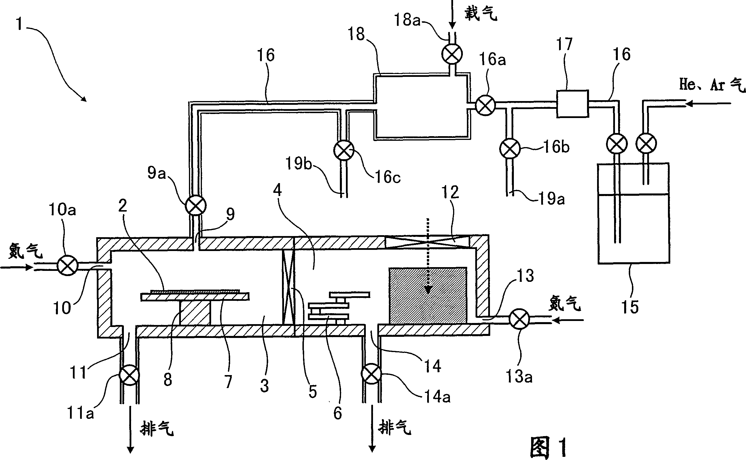
[0035] Embodiments of the present invention are described below with reference to the drawings.

[0036] First, the vapor phase cleaning treatment in the semiconductor device manufacturing method of the present invention will be described. In the present invention, gaseous carboxylic acid (RCOOH, where R=H; C N h 2N+1 、C N h M x 2N-M+1 , wherein N and M are natural numbers, and X=F, CL) reduce copper oxides such as copper oxide and cuprous oxide produced on copper electrodes and leads.

[0037] Carboxylic acid can act on copper oxide as a reducing agent, that is, carboxylic acid can reduce copper oxide to metallic copper (Cu) and generate carbon dioxide (CO 2 ) and water (H 2 O). For example, if formic acid (HCOOH) is used as carboxylic acid, copper oxide and cuprous oxide can be reduced to metallic copper, and the chemical reaction formulas are respectively and .

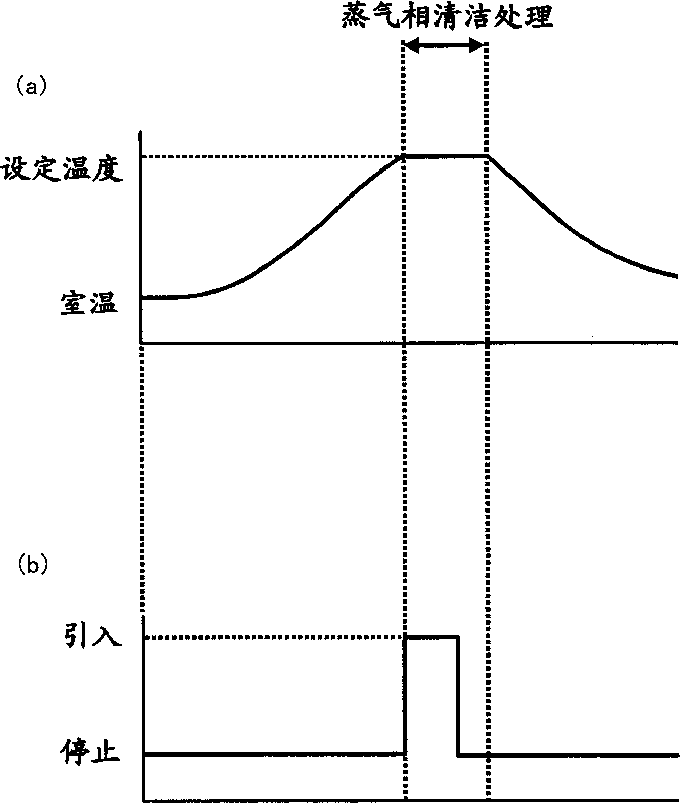
[0038] If the H produced according to the above reaction 2 O is gaseous, and the reaction s...


PUM


Abstract

A semiconductor device production method that is used to uniformly and efficiently reduce metal oxides produced on metal (copper, for example) which forms electrodes or wirings on a semiconductor device. An object to be treated on which copper oxides are produced is put into a process chamber and is heated by a heater to a predetermined temperature. Then carboxylic acid stored in a storage tank is vaporized by a carburetor. The vaporized carboxylic acid, together with carrier gas, is introduced into the process chamber via a treating gas feed pipe to reduce the copper oxides produced on the object to be treated to metal copper. As a result, metal oxides can be reduced uniformly without making the surfaces of electrodes or wirings irregular. Moreover, in this case, carbon dioxide and water are both produced in a gaseous state. This prevents impurities from remaining on the surface of copper.

Description

technical field [0001] The present invention relates to a semiconductor device manufacturing method and a semiconductor device manufacturing device, in particular to a semiconductor device manufacturing method and a semiconductor device manufacturing device for performing cleaning treatment for reducing metal oxides formed on metal electrodes or wires constituting a semiconductor device. Background technique [0002] Generally, aluminum is widely used as a material for upper electrodes and leads of semiconductor devices. In recent years, however, the increasing demand for miniaturized semiconductor devices and high-speed processing methods has made it very difficult to form such electrodes and leads using aluminum. Research has been carried out to this end, and copper has been tried to be used as a material that can replace aluminum in the next generation. Copper can withstand electromigration and has a lower resistance value. [0003] If copper is used as a material for e...

Claims


Application Information

Patent Timeline
Patent Type & Authority Applications(China)
IPC IPC(8): H01L21/302B08B7/00H01L21/00H01L21/02H01L21/306H01L21/3065H01L21/321H01L21/3213H01L21/768
CPCH01L21/67028H01L21/76814H01L21/76807H01L21/76838B08B7/0057Y10S438/906B08B7/00H01L21/02063H01L21/32135H01L21/02074H01L21/304
Inventor 埃德·A·阿克巴尔大场隆之
Owner SOCIONEXT INC
Why Eureka
Try Eureka