High reliable touch screen and manufacturing technique
A manufacturing process and touch screen technology, applied in instruments, computer parts, graphics reading, etc., can solve the problems of low square resistance uniformity of the electric film, affecting the accuracy and reliability of touch positioning of the touch screen, etc., so as to improve the square resistance uniformity , avoid deformation, and improve reliability
- Summary
- Abstract
- Description
- Claims
- Application Information
AI Technical Summary
Problems solved by technology
Method used
Image
Examples
Embodiment 1
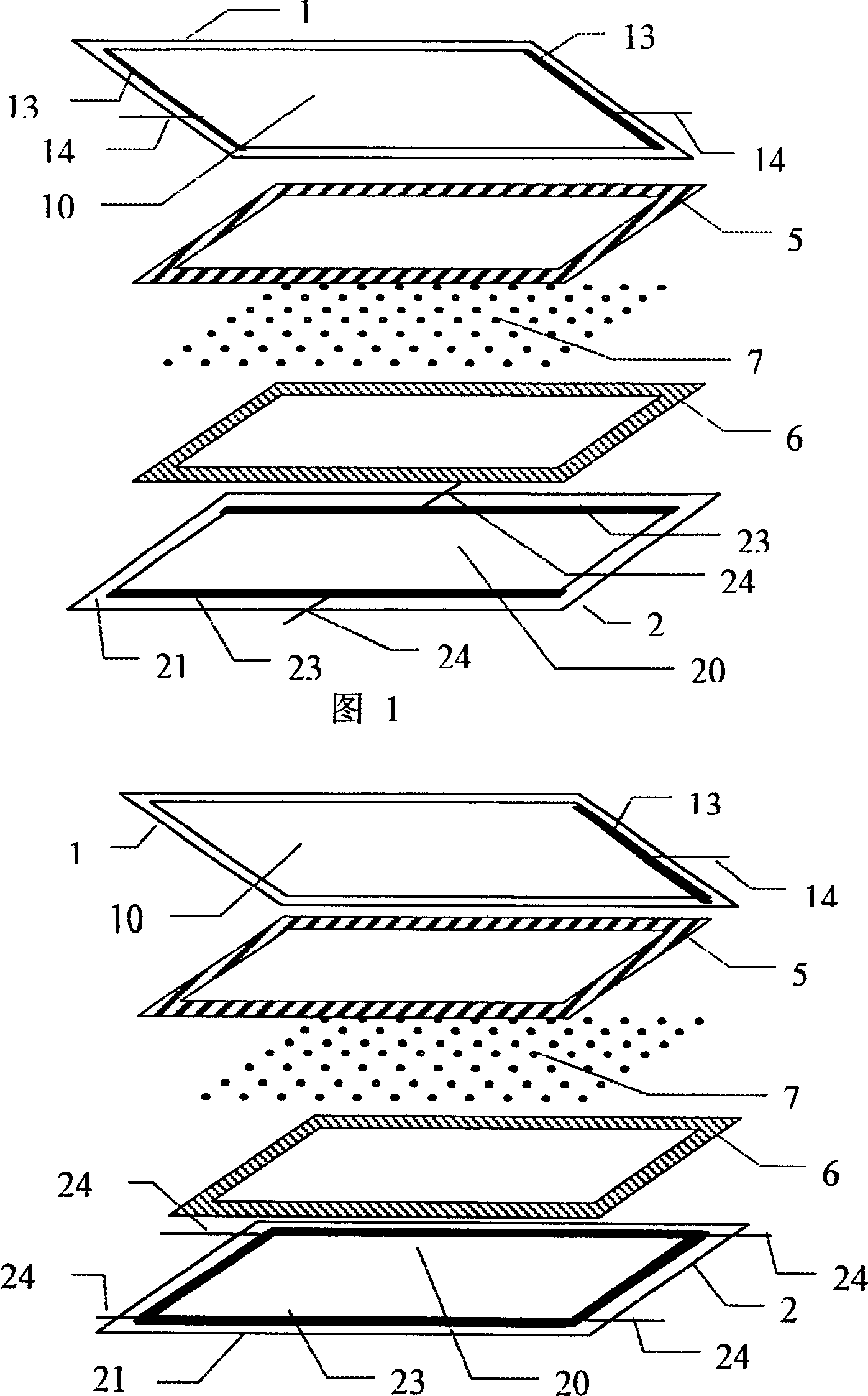
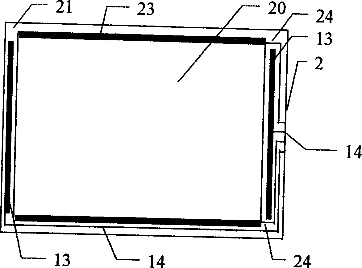
[0017] like image 3 As shown, in the conventional four-wire resistance analog touch screen of FIG. 1 , there are two pairs of orthogonal upper and lower screen electrodes 13 and 23 , which are respectively fabricated on the conductive films 10 and 20 of the upper screen 1 and the lower screen 2 . Since a pair of electrodes 13 are fabricated on the transparent resin film of the upper screen, they are generally fabricated by curing silver paste at a low temperature (generally not higher than 120° C.). In this embodiment, as image 3 As shown, the electrode 13 of the upper screen and all the lead wires 14, 24 of the upper and lower screens are all made on the area 21 where the lower screen does not have an ITO conductive film, and are insulated from each other; the electrode 23 of the lower screen is still made in the lower screen. on the membrane 20. The thickness of the electrode 13 of the upper screen is slightly larger than the total thickness of the electrode 23 of the lo...
Embodiment 2
[0019] like Figure 4 shown, with figure 2 Compared with the traditional five-wire resistance analog touch screen, in this embodiment, the electrodes 13 of the upper screen and all the lead wires 14 and 24 of the upper and lower screens are made on the area 21 of the lower screen without the ITO conductive film, and are insulated from each other; The electrodes 23 of the screen are still made on the conductive ITO film 20 of the lower screen. The thickness of the electrode 13 of the upper screen is slightly larger than the total thickness of the electrode 23 of the lower screen and the insulating layer 6, and all electrodes and electrode leads are sintered at high temperature with the high-temperature sintered silver paste as in Example 1. Then, the insulating layer 6 and the spacer lattice 7 are made of low temperature curing or ultraviolet curing material, and then the upper and lower screens 1 and 2 are sealed by the sealing glue 5 . The electrodes 13 of the upper screen ...
Embodiment 3
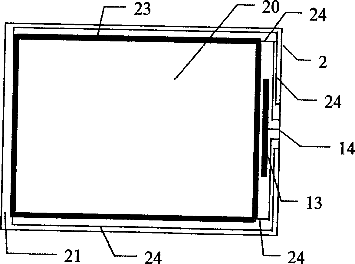
[0021] like Figure 5 As shown, this is an example of a six-wire resistive analog touch screen embodiment. In this embodiment, the electrodes 13 and the corresponding lead wires 14 of the upper screen of the two six-wire resistance analog touch screens that should have been fabricated on the upper screen 1 are all fabricated together with the electrode lead wires 24 of the lower screen. There is no ITO conduction on the lower screen. The electrodes 23 of the lower screen are still formed on the conductive ITO film 20 of the lower screen. The thickness of the electrode 13 of the upper screen is slightly larger than the total thickness of the electrode 23 of the lower screen and the insulating layer 6, and all electrodes and electrode leads are sintered at high temperature with the high-temperature sintered silver paste as in Example 1. Then, the insulating layer 6 and the spacer lattice 7 are made of low temperature curing or ultraviolet curing material, and then the upper and...
PUM
 Abstract
Description
Claims
Application Information


