High speed silicon etching method

A high-speed, corrosive gas technology, used in discharge tubes, electrical components, circuits, etc., to solve problems such as insufficient corrosion rate

Inactive Publication Date: 2003-11-26
TOKYO ELECTRON LTD +1
View PDF0 Cites 7 Cited by
  • Summary
  • Abstract
  • Description
  • Claims
  • Application Information

AI Technical Summary

Problems solved by technology

[0006] However, even if high-speed etching is performed using the existing inductively coupled plasma etching equipment, the etching rate can only reach about 10 μm / min, which cannot fully satisfy the corrosion rate.

Method used


Image

  • High speed silicon etching method
  • High speed silicon etching method
  • High speed silicon etching method

Examples


Embodiment Construction

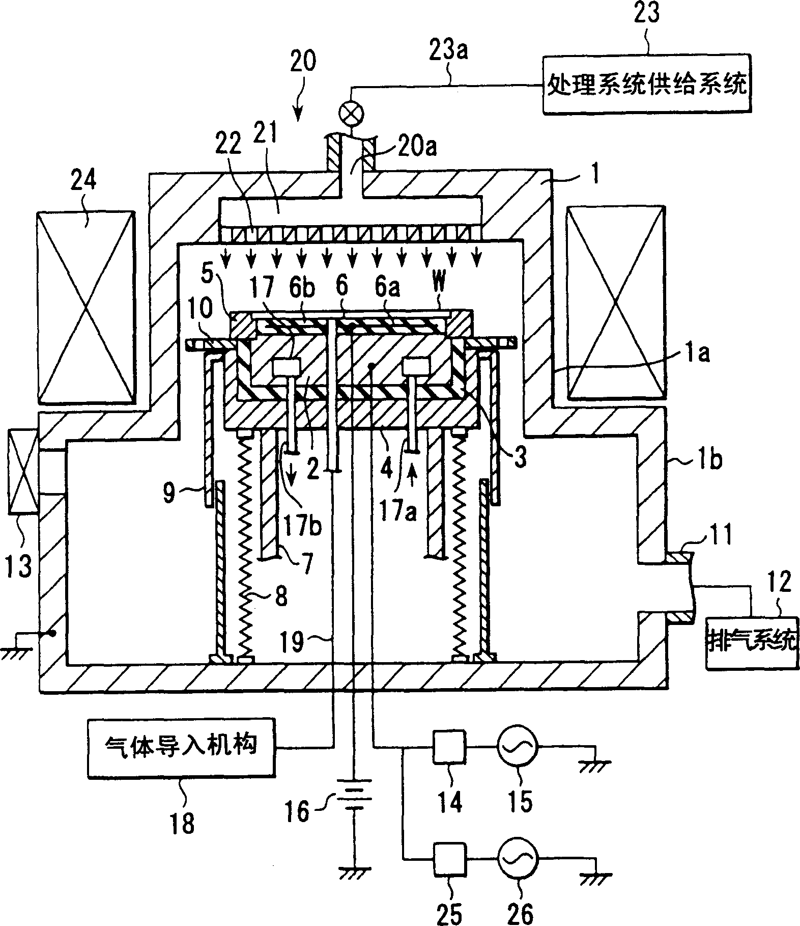
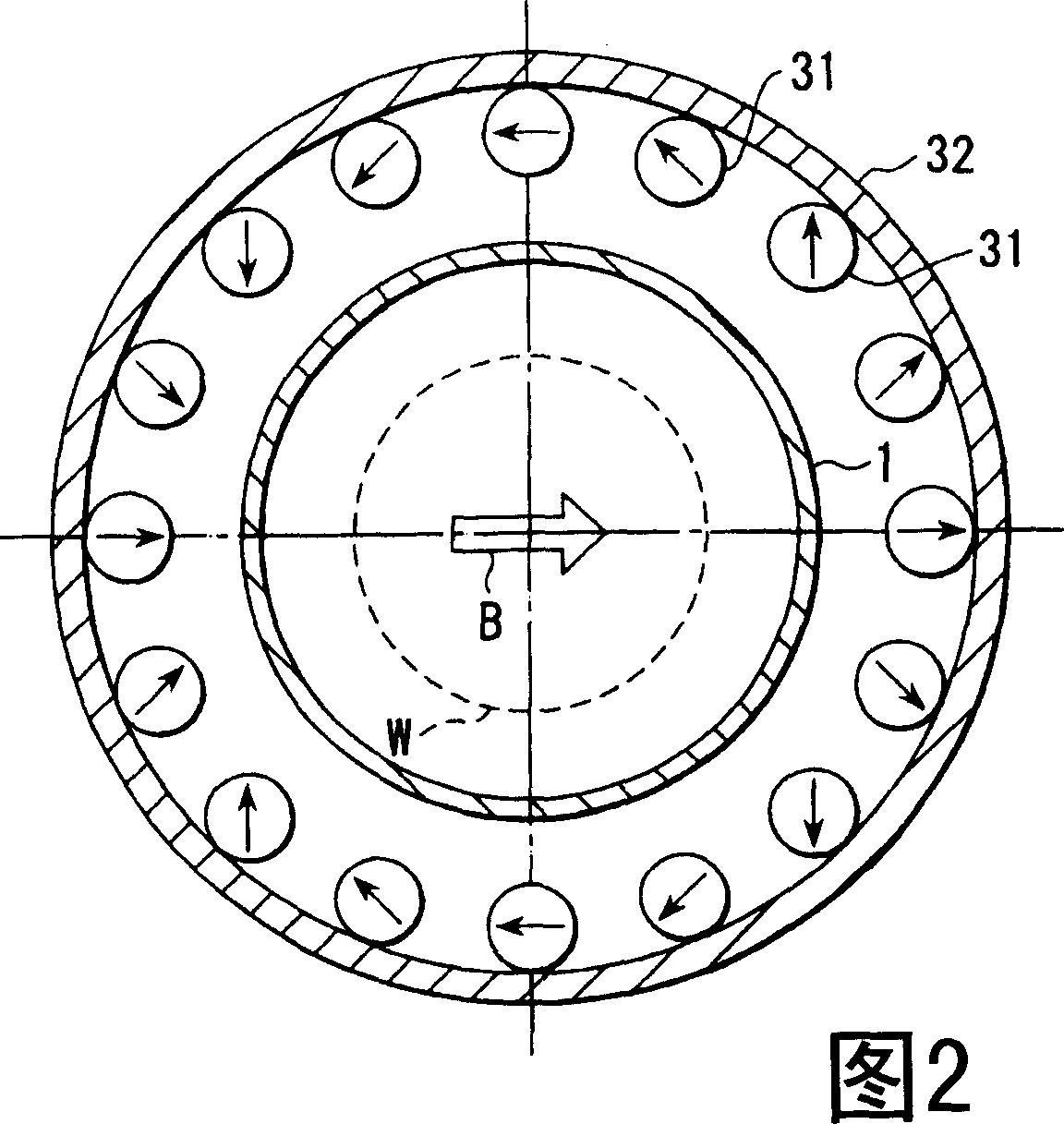
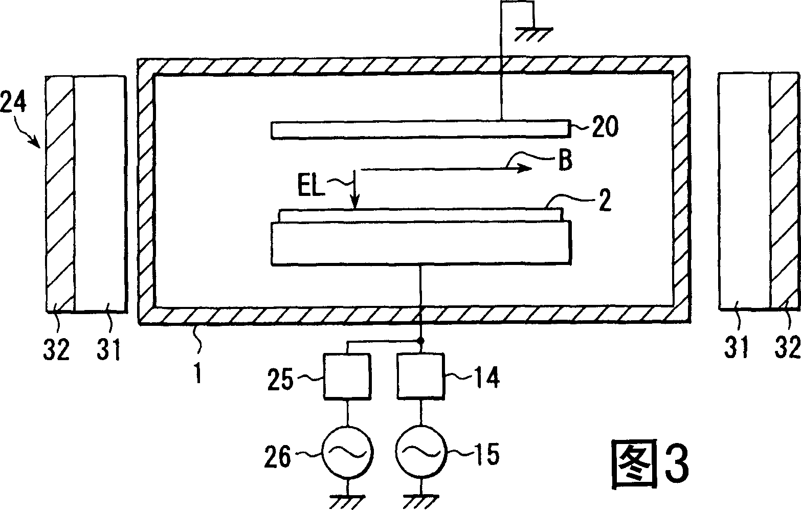
[0019] First, the concepts related to the silicon (Si) high-speed etching method of the present invention will be described.

[0020] Conventionally, high plasma density was required for high-speed silicon etching, and silicon etching was performed at high plasma density using an inductively coupled plasma etching processing device. This is to increase the plasma density, that is, to increase the plasma velocity to increase the number of ions per unit volume.

[0021] The results of this discussion, as follows Figure 4 As shown, it can be seen that in order to increase the etching rate of silicon, it is more effective to increase the gas pressure in the processing chamber than to increase the plasma density. That is, it has been found that groups that contribute to the corrosion of silicon as neutral particles increase. In order to achieve high-speed etching, the sum of the number of charged particles such as ions and the number of groups is required to be large. Therefore,...


PUM

PropertyMeasurementUnit
sizeaaaaaaaaaa
thicknessaaaaaaaaaa
diameteraaaaaaaaaa

Abstract

A high speed silicon etching method, comprising the steps of installing a processed body (W) with a silicon area in contact with a processing space in a processing chamber holdable in a vacuum, leading etching gas into the processing chamber to generate a gas atmosphere with a gas pressure of 13 to 1333 Pa (100 mTorr to 10 Torr), and applying a high frequency power to the gas atmosphere to generate a plasma, whereby a silicon area etching speed can be more increased because the sum of the quantity of charged particles such as ions and the quantity of radicals are increased in the plasma.

Description

technical field [0001] The invention relates to a silicon high-speed etching method for high-speed etching of a silicon region of a processing object such as a single crystal silicon substrate. Background technique [0002] Recently, 3-dimensional mounting devices with a multilayer structure are being developed. Such a three-dimensional mounting device is configured, for example, by stacking silicon substrates on which circuit cells and memory cells are formed in layers to form a multilayer substrate, and connecting these layers through via wiring. With this structure, a device with high space utilization efficiency can be manufactured in miniaturization. [0003] Since the three-dimensionally mounted device described above needs to form wiring via holes with a diameter of approximately 10 to 70 μm on a silicon substrate with a thickness of approximately 100 μm, extremely high-speed etching is required. [0004] In addition, the high-speed etching of silicon is not only ap...

Claims


Application Information

Patent Timeline
Patent Type & Authority Applications(China)
IPC IPC(8): H01L21/302H01J37/32H01L21/3065H01L21/308H01L21/3213
CPCH01J2237/3347H01J37/3266H01L21/32137H01L21/3081H01J37/32165H01J37/32091H01L21/3065H01J37/32082H01L21/302
Inventor 三村高范永关一也酒井伊都子大岩德久
Owner TOKYO ELECTRON LTD
Why Eureka
Try Eureka